eISSN: 2574-9927


Research Article Volume 2 Issue 3
1Crystal Growth Centre, Anna University, India
2Manonmanium Sundaranar University, India
Correspondence: Surender S, Crystal Growth Centre, Anna University, Chennai, Tamil Nadu, India
Received: April 18, 2018 | Published: May 21, 2018
Citation: Surender S, Pradeep S, Prabakaran K, et al. Growth and fabrication of InGaN metal–semiconductor–metal (MSM) photodiode. Material Sci & Eng. 2018;2(3):67-70. DOI: 10.15406/mseij.2018.02.00037
MOCVD grown InGaN/GaN heterostructure based metal semiconductor metal photodiodes fabricated with Ni/Au semitransparent electrodes by photolithography technique. The composition of the InGaN (16%) layer calculated using High Resolution X-ray Diffraction. AFM studies indicated reduced dislocation density of the epilayers. I-V characteristic studies of the photodiodes with and without illumination confirmed that, while applying bias voltage the photo generated charge carriers was more under the illuminated (2 and 4 mW/cm2) conditions and it is found to be in the order of 10-4A. Noise rejection ability of the photodiode was investigated using PC/DC ratio and a maximum value of 44 at 1.35V was obtained.
Keywords: photodiode, photocurrent, semiconductor surface, bandgap tunability
GaN, gallium nitride; LED, light emitting diode; InGaN, indium gallium nitride; MOCVD, metal organic chemical vapor deposition; HRXRD, high resolution x-ray diffraction; PL, photoluminescence; AFM, atomic force microscope; SEM, scanning electron microscope; MSM, metal semiconductor metal; FET, field effect transistor; I-V, current vs voltage.
The direct bandgap and wurtzite crystal structure of III-nitrides together with their bandgap tunability covering a wide area of electromagnetic spectra, credits these semiconductors as potential materials for energy and optoelectronic applications such as LEDs, photovoltaics, sensors and photodiodes.1–6 Photodiodes and photodetectors find applications in various commercial, military, medical, communication and space applications. The light to electricity conversion efficiency highly depends on the dislocation density and conductivity of the epitaxial layers. A photodiode is basically a p-n junction where light absorption leads to charge carrier formation at the depletion region and efficient charge separation due to the inbuilt electric field. Elemental semiconductors based photo diodes such as Si-photodiode has the limitation due to its low bandgap.7 Using III-Nitride materials high performance solid state photodiode device can be fabricated to work in UV-Visible region. Among the various III-N based photodiodes such as p-n diodes, p-i-n diodes and Metal- Semiconductor-Metal (MSM) photodiodes8 MSM photodiode have many practical applications. Generally MSM photodiodes contains two conducting electrodes (Schottky contacts) and one semiconductor surface. During operation a bias voltage is applied and MSM photodiode is irradiated under UV-visible light. Photo-generated charge carriers are generated, separated and collected by the electric field and flows as photocurrent through an external circuit.9 The MSM photodiodes has low intrinsic capacitance and compatible with FET based electronic fabrication. GaN MSM photo detectors can be easily integrated with GaN-FET devices in order to realize the III-N based optoelectronic integrated circuits.10 In comparison with the studies on III-N based LEDs and photovoltaics, relatively less research has been conducted on the photodiode/detector applications of III-nitrides which is the motivation for the current work. InGaN/GaN heterostructure has been proposed by various studies as a potential material system for photodiode fabrication. In this study we report the fabrication of MOCVD grown InGaN/GaN heterostructure based MSM photodiode using standard lithography process and its characterizations and photo response measurements. This MSM photodiode has significant performance in photocurrent measurement when compared to many previous reports.
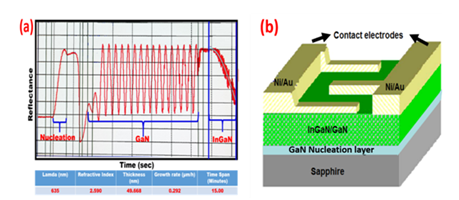
InGaN/GaN heterostructure were grown by Metal Organic Chemical Vapour Deposition (MOCVD) technique on sapphire substrate. Initially 2 inch c plane sapphire substrate was loaded in a horizontal flow MOCVD reactor system. Trimethylgallium (TMGa), Triethylgallium (TEGa) were used as gallium precursor, Trimethylindium (TMIn) as indium precursor and ammonia (NH3) as nitrogen source. Initial desorption of substrate at 1050°C was followed by the growth of 30 nm low temperature GaN nucleation layer at 500°C for 6 minutes with a reactor pressure of 200 mbar. The nucleation layer was then subjected to recrystallization process for 1 minute at 1010°C so as to improve the crystalline quality. Subsequently un-doped GaN (U-GaN) layer was grown on top of it at 1020°C for 40 minutes. Finally 50 nm InGaN layer were deposited on the U-GaN (~2 µm) layer at 720oC for 15 minutes. Using insitu-reflectance measurment (Figurre 1A) the thickness (~50 nm) and growth rate of the InGaN (0.292µm/h) layers were calculated. MSM photo dodes were fabricated by photolithography process with semitransperant Ni/Au electrodes and the schematic representation is shown in Figure 1B.

The fabrication process of InGaN/GaN MSM Photodiodes is as follows: earlier to the deposition of Ni/Au contact electrodes, the native oxides of the grown film were removed using diluted hydrochloric and distilled water solution (1:1 ratio) for 5 minutes. A Ni layer was deposited on the samples surface using E-bean evaporator. Slandered etching and lithography process were employed to define the integrated contact pattern. The active area of the whole device was 250x250µm2 and the length and breadth of the electrodes were 250 and 10µm respectively. Finaly the bonding pad Au electrode was deposited on top of the Ni contact electrodes. An I-V probstation and Keithly (Model: 2250) source meter was used to measure the current-voltage cherecteristic of fabricated MSM photodiodes in the dark and under illimination.
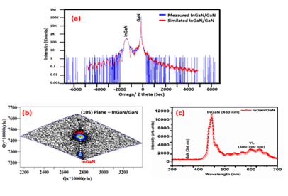
The crystalline quality of the InGaN/GaN heterostructured samples were analyzed using HRXRD measurements. Figure 2A shows the omega-2 theta scan of the 002 plane. The blue line indicates the experimental value and the red line indicates the simulated value. The simulations were carried out using epitaxy smooth fit software. Using this simulation and experimental data the thickness and composition of the InGaN layers were calculated as 50 nm and 16% respectively. The thickness value matched well with the insitu reflectance measurement studies.
In the Figure 2A the high intensity peaks corresponds to the thick GaN (002) buffer layer whereas the broad and less intensity peaks at lower angle side represents the InGaN (002) layer.11 From the figure well resolved InGaN peak was observed and the FWHM of the InGaN layer was estimated to be 382 arc.sec, which indicates good structure quality and abrupt interface between GaN and InGaN layer.
The reciprocal space mapping of the grown samples were taken using the same HRXRD measurement system in the off axis (105 plane) (Figure 2B). The RSM studies confirms that InGaN epilayer were epitaxialy grown on GaN buffer layer without any relaxation. This result indicates that InGaN is pseudomorphicaly grown on GaN layer. Figure 2C shows the photo luminescence spectrum of as grown InGaN/GaN heterostructure under 244 nm excitation. The peak at 364 nm corresponds to band to band optical transition of the GaN bufferlayer. Peak appears at 450 nm due to band edge emissions of InGaN. The defect level emission or Yellow Luminescence (YL) appears from 500 nm to 700 nm, which are attributed to Ga or N vacancy.

Figure 3A shows the cross-sectional Scanning Electron Microscopy (SEM) image of the as grown InGaN/GaN heterostructure. The thickness of the InGaN layer was found to be 50 nm and it was well matched with HRXRD omeg-2 theta measurement. The morphological analysis of the sample was carried out using the non-contact mode AFM in 2x2µm2 scan area as shown in Figure 3B. This study confirms that the surface morphology have spiral growth mechanism with average roughness of 0.52 nm. Generally it is very dificult to grow good quality of InGaN layer on sapphire due to the lattice mismatch between them which leads to high defect density in the order of 109/cm2. In order to reduce the mismatch and dislocations, InGaN layer was grown on thick GaN layer.10 The screw type dislocations of the grown InGaN sample was calculated as 8.2 x10⁷/cm2 wich shows that dislocation density is reduced by two order of magnitudes. A reduced dislocation density is highly advisable for photodiode applications since dislocations can act as charge carrier traps leading to recombination of photogenerated charge carries, affecting the device performance. AFM image clearly shows the fewer amount of screw type dislocations, these kind of screw dislocation originates from GaN and InGaN interfaces due to the lattice missmatch between GaN and InN .

After the fabrication of InGaN/GaN MSM photodiode device was subjected to electrical characterizations. Figure 4A shows the I-V characteristics InGaN/GaN MSM photodiodes with and without illumination. It can be seen that the photo current was high compare with the dark current. From the I-V plot (Figure 4A) it is evident that the photo current of the MSM InGaN/GaN photodiodes linearly increasing with the applied bias voltage. While increasing the power of the illuminating light source the photocurrent also increases gradually because the generated electron-hole pairs also increases. The observed dark current is attributed to lower Schottky barrier height between metal contacts and InGaN. The nitrogen or gallium vacancy (Yellow Luminescence) and surface defects like screw dislocation which were shown in PL and AFM respectively, also could be a reason for the observed dark current in the InGaN MSM photodiodes. Under illumination InGaN MSM photodiode generates large amount of photo-generated charge carrier, therefore when external voltage is applied to the device the photocurrent increases due to increased charge carrier separation. Figure 4B shows the dark and photo current measurement in logarithmic scale. It clearly explains in the range of 0-1.35 volts there is a large amount of photocurrent generated under illumination.
The Photo Current (PC) to Dark Current (DC) ratio clearly explains about the noise-rejection ability of photodiodes.12 PC/DC ratio of the MSM InGaN/GaN photodiode of two different illuminations shown in Figure 4c, which shows that higher PC/DC ratio values obtains at lower voltages range (below 1.5V) compared to higher voltage range. The higher PC/DC ratio value at lower voltage is due to the lower values of dark current. Further increasing voltage beyond 4V the ratio of PC/DC was saturated and independent to applied voltage. The highest PC/DC ratio values obtained were 44 and 13 for 4 mW and 2 mW illuminations respectively (at 1.35V). This is a significant performance when compared to many previous reports.12
In summary, InGaN/GaN heterostructure was grown on sapphire substrate using horizontal flow MOCVD reactor system. The composition thickness and crystalline quality of the grown sample were characterized using HRXRD and PL. The spiral growth mechanism of the InGaN/GaN layer was observed and explained using AFM studies. InGaN/GaN MSM photodiode was successfully fabricated using photo lithography and the I-V characteristics were recorded. The photocurrent measurements showed photodiode generates high photocurrent in the order of 10-4 A under illuminated conditions. Noise rejection ability of the photodiode investigated using PC/DC ratio showed a maximum value of 40 for 4 mW illumination at 1.35V.
The authors gratefully acknowledge the financial support by the Department of Science and Technology (DST/TM/SERI/2k12/71(G)), India. The first author (S. Surender) would like to thank UGC- RGNFSC, Govt. of India for the award of Senior Research Fellowship (F1-17.1/2015-16/RGNF-2015-17-SC-TAM-5892).
Author declares there is no conflict of interest.

©2018 Surender, et al. This is an open access article distributed under the terms of the, which permits unrestricted use, distribution, and build upon your work non-commercially.