eISSN: 2641-936X


Mini Review Volume 1 Issue 1
Department of Electrical & Computer Engineering, University of Alberta, Canada
Correspondence: Masum Hossain, Department of Electrical & Computer Engineering, University of Alberta, Canada, Tel 780-492-693-6
Received: June 19, 2017 | Published: July 19, 2017
Citation: Hossain M. Recent trend in high-speed wireline link design. Electric Electron Tech Open Acc J. 2017;1(1):16-18. DOI: 10.15406/eetoaj.2017.01.00004
This short article provides a brief summary of the current status of high speed wireline links and its future trend. It also captures the motivating factors for recent changes and explains the fundamental reasons behind it. Lower SNR in multilevel modulation has motivated recent change in the link architecture developed in leading R & D groups and differentiating features. Lastly, it points out the challenges to motivate future research work in academia and industry.
Keywords: wireline, inter-symbol-interference, modulation
ISI, inter symbol interference; CTLE, continuous time linear equalization; DFE, decision feedback equalization; FFE, feed-forward equalization
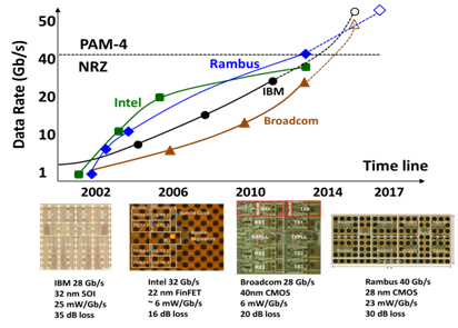
We are at a historical cross road in technology roadmap where the numbers of objects connected through internet have vastly outnumbered the human network. This network of smart objects, also known as IoT, will shape our life in the next decade and beyond. By 2020, the number of smart objects is expected to reach 100 million sending massive information over internet. To accommodate such user demand, data centers are also evolving both electrical and optical links are adopting complex modulation schemes. Eventually the need for higher speed from the users, service provider and equipment manufacturer motivates the researchers to push the limit of semiconductor device physics and communication theory. Ultimately, the end product is a fully integrated monolithic solution capable of transmitting and receiving terabits of information. Few example of such market driven R & D development efforts are given in Figure 1. While the particular development trend in each company may vary based on their business strategy, one consistent trend is the rapid increase in data rate over time. Figure also includes example work from these efforts and that also capture underline motivating factors:

Figure 1 Trend in High speed Link development in leading research and development groups in the world. Below is the example demonstration developed hardware solution with performance summary.
Over last two decades wire-line channels have evolved drastically to overcome high frequency losses. High frequency loss causes the transmitted symbols to disperse which results in inter-symbol-interference (ISI). The techniques to reduce these ISI components are known as equalization. The recent advances in interconnect technology and development of low loss dielectric such as Megatron have significantly extended their reach. This improvement in channel along with advances in equalization techniques have enables 100 Gb/s Ethernet. Improving the loss characteristics of channel increases system cost as shown in Figure 2. However, industry is facing an inevitable challenge despite using expensive lowest loss material and high quality connectors, only few 10s of cm channels suffering 45 dBs of loss @ 25 GHz. Such channel loss causes significant inter symbol interference (ISI), and existing equalization techniques are proving to be insufficient to compensate that. Unfortunately, this also aligns with the end of Moore’s law; therefore, we can no longer rely on higher performance devices to overcome the challenges. This creates an opportunity for disruptive technology and architecture.
In high-speed wireline transceivers, the frequency dependent channel loss is the main source of inter-symbol interference (ISI). In simple word, ISI is the residue of the current symbol that affects the following symbols (pre-cursor) as well as the previous symbols (post-cursor). For high loss channel, conventional receiver designs usually feature analog linear equalization techniques such as continuous time linear equalization (CTLE) and passive equalization at the front end as shown in Figure 3. In addition, decision feedback equalization (DFE) and feed-forward equalization (FFE) techniques are used for further ISI cancellation and bit detection. Fundamentally, this limitation is coming from degradation of low signal-to-noise and signal-to-crosstalk ratio that is unavoidable in existing equalization techniques. Analog mixed-signal solution in general can equalize with excellent energy efficiency (around ~3pJ/bit).3 But these solutions have their limitations: first, SNR degradation CTLE that generally inverts the channel also amplifies noise, including crosstalk noise and degrades SNR. Second, the linearity requirement scaled supply reduces maximum achievable linear swing. Third, process variation makes it very difficult to achieve reliable control over zero and pole frequencies to achieve the desirable frequency response. All these factors limit the performance of existing equalization techniques and ultimately our demonstrated capability of equalization is limited to 40 dB (Figure 4).
The equalization becomes more complicated when we move to higher order modulation as PAM-4 for several reasons
All these challenges motivate us to rethink the equalization strategy as well as receiver architecture. Recently ADC based architectures are gathering interest to enhance performance through digital processing. Therefore, in ADC based receivers where equalization is done digitally, can take advantage of the technology scaling, enables advanced equalization that can compensate higher loss compared to traditional mixed signal equalization. However, the challenge in this architecture is the front-end ADC that consumes significant power to provide the required resolution. When compared to traditional mixed signal receiver, ADC based solutions’ power consumption is 2x higher.6-13 Fortunately, recent trend is to improve their energy efficiency significantly, most of those are enabled through academic research and development that allows flexibility for disruptive approaches (Figure 5). Given the strict energy efficiency target, application of ADC based links depends on successful adoption of these techniques.
None.
The author declares no conflict of interest.

©2017 Hossain. This is an open access article distributed under the terms of the, which permits unrestricted use, distribution, and build upon your work non-commercially.