Research Article Volume 2 Issue 1
Numerical method for a one dimensional defective photonic crystal selective filters
Ouarda Barkat,
Regret for the inconvenience: we are taking measures to prevent fraudulent form submissions by extractors and page crawlers. Please type the correct Captcha word to see email ID.

Badreddine Mamri
Department of Electronics, University Frères Mentouri Constantine, Algeria
Correspondence: Ouarda Barkat Department of Electronics, University Frères Mentouri Constantine, Algeria
Received: June 27, 2017 | Published: April 17, 2018
Citation: Barkat O, Mamri B. Numerical method for a one dimensional defective photonic crystal selective filters. Electric Electron Tech Open Acc J. 2018;2(2):9-13.
DOI: 10.15406/eetoaj.2018.02.00014
Download PDF
Abstract
In this work, we demonstrate via numerical simulation the general design for one dimensional defective photonic crystal (1D- DPC), the defect was fictionalized with two different dielectric layers. In the design procedure, the transfer matrix method is used to determine the transmission coefficient for both TE (Transverse Electric) and TM (Transverse Magnetic) modes. Then, we focused point on a special class of optical elements, namely selective filters. Simulation results obtained showing the number of defect mode within the photonic band gap (PBG) in the asymmetric (1D- DPC) structure, more than in the symmetric (1D- DPC) structure. The dependences of defect modes on the angle of incidence are illustrated.
Keywords: photonic band gap, transfer matrix method, defect mode, transmission, dispersion
Introduction
The one dimensional photonic crystal (1D-PC) structures have become attractive to optical engineering due to its several beneficial features, such as its ability to control and manipulate the propagation of electromagnetic waves in limited space.1 These structures have a number of useful properties, which are employed as low-loss optical waveguides, dielectric reflecting mirrors, optical switches, optical limiters, and optical filters etc.2–4 It has been demonstrated experimentally and theoretically that (1D-PC) structures have complete omnidirectional photonic band gaps (PBGs).5 Therefore it is possible to create pass bands within the photonic band-gap by introducing of defects layers. When a defect layer is inserted into a one dimensional photonic crystal, localized defect mode will be appeared in the photonic band gaps (PBG), which are much more similar to the defect states generated in the forbidden band in a doped semiconductor. Recently, the defect modes inside the photonic band have been widely studied due to their properties.6–10 The perfect layer can be realized, by changing physical parameters, such as changing the thickness of one of the layer, adding another medium to the structure, or removing a layer from (1D-PC) structures. The localized defect modes, which are also called resonant transmission peaks, can be generated within the PBG due to the change of the interference behavior of light. The defect models properties can be used to make high quality extremely narrowband frequency selective filters.7–11 Selective photonic crystal filters have received much research interest in the fields of demultiplexers for WDM systems.12 Nowadays, the numerical modeling of photonics crystals is based on the calculation of the transmission, and the reflection coefficient properties. These methods including the plane wave expansion (PWE) method, the generalized Rayleigh identity method, the finite-difference time-domain (FDTD) method, and the transfer matrix method (TMM). Each method has its own limitations for finding some important properties of one dimensional defective photonic crystal (1D-DPC). The transfer matrix method is most popular because of its simplicity in algorithm and capability to model complex structures.13,14 It is recently introduced by Pendry and MacKinnon, to calculate the electromagnetic transmission through the PBG materials.15 In this paper, the transmission spectrum was obtained by applying the transfer matrix formalism to one dimensional defective photonic crystal (1D-DPC). The effects of the polarization and the angle of incidence on the defect modes in the transmission spectra are investigated. Several simulation cases by Matlab will be given to show the performance of this approach. The accuracy of the analysis is tested by comparing the computed results with measurements published data.
Theory
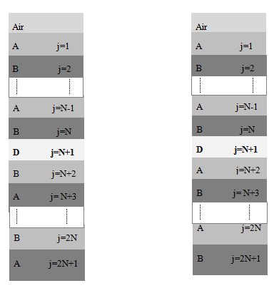
Let us consider first the (1D-PC) structure consisting of alternating multilayer of the form (AB)ND (AB)N and (AB)ND (BA)N shown in Figure 1, there are 2N+1 layer made up of dielectric materials A and B, and dielectric defect layer D. Each layer has to be dl thicknesses, and refractive index nl. In order to find the formulation of the structure, we supposed that the incident electromagnetic wave from air to In As and SiO2 medium. Let the layers be in the x-y plane, the z direction being normal to interface of layers.

Figure 1 Structure of one-dimensional photonic crystal containing a defect.
Symmetric defective (1D- DPC); Asymmetric defective (1D- DPC)
The refractive index profile of considered structure can be given as
(1)
And
(2)
Where
L, is number of layer
, is period
Based on the Maxwell equations and the boundary conditions, the TMM has been widely used to calculate the amplitude and phase spectra of the light wave propagating in a (1D- PC) structure. We are going to suppose that a space time dependence of all the components of the kin
. The transverse components of the E and H fields from Maxwell’s equations in the lth layer, for TM polarization, are given by:
(3)
(4)
(5)
Where Al and Bl are the amplitudes of the forward and backward travelling waves in the lth layer.
The transverse components of the E and H fields from Maxwell’s equations in the lth layer, for TE polarization, are given by:
(6)
(7)
(8)
Where the wave numbers and intrinsic impedances are:
(9)
(10)
When an electromagnetic wave propagates in (1D- PC) structure, the incident, reflected and transmitted electric fields are connected via the transfer matrix M. By using the boundary conditions and the condition of continuity of E and H fields at the interfaces of
and
we can find out the relationship between the fields (1D- PC) structure consisting of l layer, this relation is already exposed.16
(11)
The matrix Ml-1 of the lth layer can be written in the form.17–19
(12)
and
being the matrix parameters and depending on the incident angle of light, the optical constants and the layer thickness, are expressed as:
(13)
(14)
We note that
is related to the angle of incidence
by the Snell’s Descart’s low, that is
(15)
By considering the transmission matrix of each layer, we are able to obtain the transmission matrix of whole structure. For l number of multilayers; the corresponding transfer matrix can be defined as a product of matrices, is obtained for symmetric PBG structure.20,21
(16)
And for asymmetric PBG structure.
(17)
Where
MA is the transfer matrix of the first dielectric layer.
MB is the transfer matrix of the second dielectric layer.
MD is the transfer matrix of the dielectric layer defect.
These formulas can be modified by using N number of defect, are obtained for symmetric PC
(18)
Where L is number of dielectrics layers defect and dielectric layer B between the defects. And for asymmetric PC
(19)
Where m11, m12, m21 & m22 are the complex numbers
The transmittance t and reflectance r are defined as the ratios of the fluxes of the transmitted and reflected waves, respectively, to the flux of the incident wave. After some derivations, the total transmission and reflection coefficients
are given by
(20)
(21)
Here p0 and ps are the first and last medium of the structure which given as
(22)
(23)
Where
Hence the reflectance R and transmittance T spectrums of can be obtained by using the expressions:
(24)
(25)
Numerical calculation and discussion
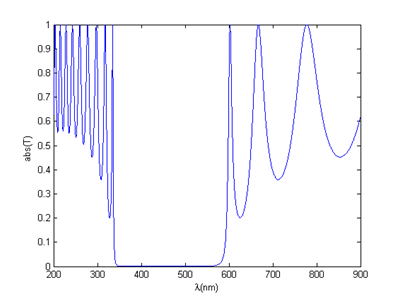
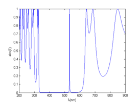
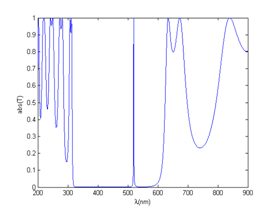
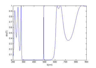
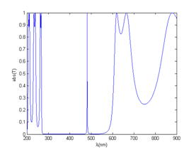
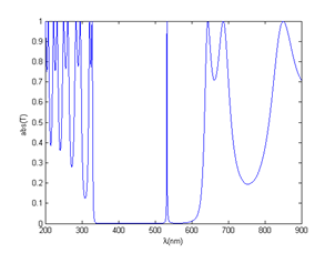
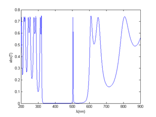
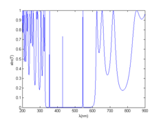
In this subsection, the transmission spectra have been calculated using the theory described in previous section. We consider only normal incidence of the electromagnetic wave on the (1D- PC) structure. The structure is restructured as (An Bn)m where n = 1 . . m, m is chosen as 8. We have kept constant the refractive index of the layers, are fixed to be nInAs = 3.3842, and nSiO2 = 1.4672 at λ=0.43µm. The layer thicknesses were taken as dSiO2 =0.0733µm, and dInAs =0.0318µm. The transmission spectra in Figure 2 is computed and plotted with wavelength centered at 550 nm. According to these results, we are able to see that the structure exhibits various band gaps (or stop band) where the photonic states are forbidden in the structure, can be seen in the transmission spectrum. Furthermore we have observed that the phonic band gap which is limited at 342.7nm to 578.3nm. In order to check the effects of the defect layer, we introduce a defect layer TiO2 with refractive index nTiO2=2.8717, and thickness dTiO2=0.0187µm, in the (1D-DPC) structures containing InAs and SiO2. The refractives index of InAs and SiO2 are nInAs=3.3842, nSiO2=1.4672, and thickness d InAs=0.0318µm, dSIO2=0.0733µm. In Figures 3, we have plotted the wavelength-dependent transmittance spectra for the symmetric and asymmetric (1D- DPC) structures. Because of the existence of defect layer, it is found that there exists a very narrow pass band or single defect mode within the photonic band gap (PBG) is observed. For the asymmetric (1D-DPC) structure with the configuration (Air/(AB)4D(AB)4/ Air), the bandwidth was calculated as ΔBwp =(601.504-332.1712) =269.3328nm, and the resonant peak locates at the design wavelength of λ=370.2nm. For the symmetric (1D- DPC) structure with the configuration (A/(AB)4D(BA)4/Air), the bandwidth was calculated as ΔBwp=(604.294-334.252)=270.042nm, the resonant peak locates at the design wavelength of λ=532.4nm. Additionally, as seen from the figures, in the asymmetric structure the defect modes appear in higher frequencies with a small amplitude compared to the symmetric structure. Accordingly, this reduction in the amplitude of the defect peak becomes more significant for the case of asymmetric structure. These behaviors agree very well with those reported by work.20–22 The effects of the polarization and the angle of incidence on the defect modes in the transmission spectra for TE or TM modes are illustrated in Figure 4, Figure5 & Table 1. We have clearly observed that the transmittance spectrum of the defect mode is linked to the angle of incidence in TE and TM modes. Also, the position of narrow pass band is changed, and width of the band increases obviously for TE mode, and decrease for TM mode. On the other hand a pick of transmission change in the direction of small values when the angle incidences increase for TM mode. As shown in Figure 4, a pick of transmission occurred at the wavelength 532.4nm when θ=0°, 519.9nm when θ=30°, 492.2nm when θ=60°, and 481.6nm when θ=75° for TE mode. As seen and extracted from the Figure 5, the variation of transmission spectra for TM mode, a pick of transmission with a weak value occurred at the wavelength 504.6 nm when θ=30°, 444.2 nm when θ=60°, and 420.8 nm when θ=75°. Moreover, for both polarizations the frequency of the defect mode is shifted to the higher frequency as the angle increases. In addition, these results reveal that as the angle of incidence increases, the peak height of the defect mode decreases for TM mode and increases for TE mode. A comparative study, between our results and those available in the literature, shows the possibilities of the adjustment of transmission spectra of InAs and SiO2 mediums in presence of TiO2.The change in the angle of incidence and the polarization allows us to obtain an adjustable defect mode.9 In Figure 6, we examine the effects of the two defect layers, by introducing two defect layer TiO2 having thickness dTiO2 = 0.0374µm, in the (1D-DPC) structure symmetric and symmetric. It is found that there exists a two defect mode within the photonic band gap (PBG) in the(1D-DPC) structure symmetric with the configuration ((Air/(AB)4DBD(BA)4/Air)), the bandwidth was calculated as ΔBwp=(613.312-331.404) =281.908nm, as well as the resonant peak locates at the design wavelength of λ1=364.9 nm and λ2=523.6nm. For the (1D- DPC) structure asymmetric with the configuration (Air/(AB)4DBD(AB)4/Air), the bandwidth was calculated as ΔBwp =(600.4 -335.3)= 265.1nm, and the resonant peak locates at the design wavelength of ¸ λ1=430.1nm. In Figure 7, we have examined the effect the effects of the tree defect layers, by introducing tree defect layer TiO2 in the (1D- DPC) structures symmetric and asymmetric. It was found that it existed a tree defect mode within the photonic band gap (PBG) in the (1D-DPC) structure symmetric with the configuration (Air/(AB)4DBDBD(BA)4/Air, the bandwidth was calculated as ΔBwp=(605.107-343.632)=261.475nm, the resonant peak locates at the design wavelength of ¸ λ1=354.9nm, λ2=429.9nm and λ3=545. 3nm. For the (1D- DPC) structure asymmetric with the configuration (Air/(AB)4DBD(AB)4/Air), the bandwidth was calculated as ΔBwp=(574.54-343.666)=230.874nm, the resonant peak locates at the design wavelength of λ1=396.8 nm and λ2=468.9nm. Our results imply that the number of defect mode can be increased by adding the layer TiO2 in structure.8
|
TE mode |
TM mode |
θ |
ΔBwp(nm) |
λ(nm) |
ΔBwp(nm) |
λ(nm) |
0° |
(604.294-334.252)= 270.042 |
532.4 |
(604.294-334.252)=270.042 |
532.4 |
30° |
( 597.66-318.9)=278.76 |
519.9 |
(579.1-325.4)=253.7 |
504.6 |
60° |
(576.5-285.9)=290.6 |
492.2 |
(518.1-306.3)=211.8 |
444.2 |
75° |
(574.4 -271.6)=302.8 |
481.6 |
(504.9-296.6)=208.3 |
420.8 |
Table 1 Bandwidth and wavelength with different the angle of incidence and polarization of Transmission spectra of (1D- DPC) structure symmetric (Air/(AB)4D(BA)4/Air), (nInAs=3.3842, nSiO2=1.4672, d InAs=0.0318µm, dSIO2=0.0733µm, nTiO2=2.8717, dTiO2 = 0.0187µm)

Figure 2 Transmission spectra of (1D- PC) structure, nInAs=3.3842, nSiO2=1.4672, d InAs=0.0318µm, dSIO2=0.0733µm.
-
(A) θ=0°,
(B) θ=30°
(C)θ= 60°, (D) θ = 75°
Figure 4 Transmission spectra of (1D-DPC) structure symmetric (Air/(AB)4D(BA)4/Air), TE mode (nInAs=3.3842, nSiO2=1.4672, d InAs=0.0318µm, dSIO2=0.0733µm, nTiO2=2.8717, dTiO2=0.0187µm).
-
(A) θ =0°
(B) θ= 30°
(C)θ= 60°, (D) θ = 75°
Figure 5 Transmission spectra of (1D- DPC) structure symmetric (Air/(AB)4D(BA)4/Air, TM mode
(nInAs=3.3842, nSiO2=1.4672, d InAs=0.0318µm, dSIO2=0.0733µm, nTiO2=2.8717, dTiO2=0.0187µm).
-
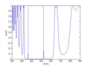
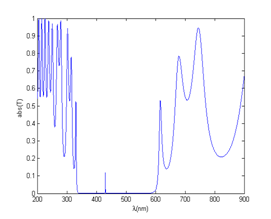
(A) Symmetric (Air/(AB)4DAD(BA)4/Air);
(B) Asymmetric (Air/(AB)4DBD(AB)4/Air)
Figure 6 Transmission spectra of (1D- DPC) structure (nInAs=3.3842, nSiO2=1.4672, d InAs=0.0318µm, dSIO2=0.0733µm, nTiO2=2.8717, dTiO2=0.0374µm, θ=0°).
-
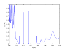
(A) Symmetric (Air/(AB)4DADAD(BA)4/Air);
(B) Asymmetric (Air/(AB)4DBDBD(AB)4/Air)
Figure 7 Transmission spectra of (1D- DPC) structure (nInAs=3.3842, nSiO2=1.4672, d InAs=0.0318µm, dSIO2=0.0733µm, nTiO2 =2.8717, dTiO2 =0.0748µm, θ=0°).
Conclusion
In summary, we have used the transfer matrix method to study one-dimensional photonic crystal defectives. We have discussed the properties of the defect modes for the asymmetric and symmetric structures for both TE and TM modes at different incidence angles. The results have shown the calculated the transmission with defects separated by different layers. When the order of the defect layer increased such as m=1, 2, 3 etc, additional modes occurs in photonic band gap. We can conclude that when the existence of defect layer, there is a very narrow pass band whose pick of transmission is observed. The maximum of transmission was obviously observed at these wavelengths for TE mode. Besides the dependence on angle of incidence of the defect mode, it has been noticed that selection of wave mode has significant effect on the peak position and amplitude of the defect mode. In other words, defect modes peak is related to the angle of incidence. For TM mode, the magnitude of transmission of the pass bands decrease for higher angle incidence. However, in TM waves, the frequency increases as the angle of incidence increases
Acknowledgements
Conflict of interest
Authors have declared no conflict of interests.
References
- Sakoda K. Optical properties of Photonic Crystals. New York: Springer Berlin Heidlberg; 2005.
- Gondek E, Karasiński P. One-dimensional photonic crystals as selective back reflectors. Optics & Laser Technology. 2013;48:438–446.
- Kumar V, Suthar B, Kumar A, et al. Silicon based one dimensional photonic crystal as a TM-mode filter. Springer science Silicon. 2014;6(1):73–78.
- Young L, Cristal EG. Low-Pass and High-Pass Filters Consisting of Multilayer Dielectric Stacks. IEEE Transactions on Microwave Theory and Techniques. 1966;14(2):75–80.
- Shadrivov V, Sukhorukov AA, Kivshar YS. Complete band gaps in one-dimensional left-handed periodic structures. Physical Review Letters. 2005;95:14.
- Ya Vetrov S, Shabanov AV, Shustitskiĭ EV. Control of the transmission spectrum of a photonic crystal with lattice defects. Optics and Spectroscopy. 2006;100(3):409–413.
- Hadjira A, Badaoui, Abri M. One-dimensional photonic crystal selective filters design using simulated annealing optimization technique. Progress in electromagnetic research B. 2013;53:107–125.
- Tang L, Gao L, Xing FJ. Characterization for defect modes of one-dimensional photonic crystals containing Metamaterials. Chinese optics letters. 2008;6(3):201–203.
- Lotfi E, Jamshidi GK, Moslem F, et al. Comparison of photonic crystal narrow filters with metamaterials and dielectric defects. The European Physical Journal D. 2010;60(2):369–372.
- Němec H, Kužel P, Garet F, et al. Time-domain terahertz study of defect formation in one-dimensional photonic crystals. OSA Publishing, Applied Optics. 2004;43(9):1965–1970.
- Gaspar JA. Photonic crystal to photonic crystal surface modes: narrow-band pass filters. Optics express. 2004;12(11):2338–2355.
- Ghoch R, Ghoch KK, Chakraborty R. Narrow band filter using 1D periodic structure with defects for DWDM systems. Optics communications. 2013;289:75–80.
- Lin MC, Jao RF, Huang KH. Transfer matrix approach to study light scattering in complex layered media. Conference Digest of the 2004 Joint 29th International Conference on Infrared and Millimeter Waves, and 12th International Conference on Terahertz Electronics. 2004.
- Oraizi H, Abdolali A. Several theorems for reflection and transmission coefficients of plane wave incidence on planar multilayer metamaterial structures. IET Microw Antennas Propag. 2010;4(11):1870–1879.
- Pendr JB, Mackinnon A. Calculation of photon dispersion. Phys Rev Lett. 1992;69(19):2772–2775.
- Scotognella F. Four-material one dimensional photonic crystals. Elsevier: Optical Materials. 2012;34(9):1610–1613.
- Xiao-Qin H, Yi-Ping C. Degeneracy and Split of Defect States in Photonic Crystals. Chinese Physics Letters. 2003;20(10).
- Kumar V, Suthar B, Kumar A, et al. Silicon Based One-Dimensional Photonic Crystal as a TM-Mode Filter. Springer Silicon. 2014;6(1):73–78.
- Villa F, Gaspar AJA. Photonic crystal to photonic crystal surface modes: narrow-bandpass filters. Optics Express. 2004;12(11):2338–2355.
- Wu CJ, Wang ZH. properties of defect modes in one-dimensional photonic crystals. Progress In Electromagnetics Research. 2010;103:169–184.
- Tameh TA, Memarzadeh BI, Granpayeh N, et al. Analysis and optimization of optical bistability in one-dimensional nonlinear photonic crystal with (HL)p(D)q(LH)p and (LH)p(D)q(HL)p structures. Elsevier Optik. 2010;121(19):1729–1734.
- Kumar V, Suthar B, Kumar A, et al. Design of a wavelength division demultiplexer using Si-based one-dimensional photonic crystal with a defect. Elsevier Optik. 2013;124(16):2527–2530.

©2018 Barkat, et al. This is an open access article distributed under the terms of the,
which
permits unrestricted use, distribution, and build upon your work non-commercially.


