Submit manuscript...
eISSN: 2641-936X

Electrical & Electronic Technology Open Access Journal

Research Article Volume 1 Issue 1

Unambiguous determination of the wave impedance of slow-wave structures

Yuriy N Pchelnikov

Pchelnikov’s Consulting, USA

Correspondence: Yuriy N Pchelnikov, Professor at Pchelnikov’s Consulting, USA

Received: April 18, 2017 | Published: June 19, 2017

Citation: Pchelnikov YN. Unambiguous determination of the wave impedance of slow-wave structures. Electric Electron Tech Open Acc J. 2017;1(1):1-5. DOI: 10.15406/eetoaj.2017.01.00001

Download PDF

Abstract

A new method of calculating the wave impedance of slow-wave structures (SWSs) based on the choice of an equivalent transmission line with decreased series inductance and increased shunt capacitance is demonstrated. It is shown that the calculation of the real conduction current in the longitudinal direction and the power flow makes it possible to find the equivalent voltage, which can be used for correcting parameters of the equivalent line. The proposed method is demonstrated using the example of a helix in the sheath approximation. Expressions for the equivalent inductance, capacitance, and voltage, which enable one to obtain the identical values of the wave impedance from all formulas of the circuit theory, are derived. Calculation of the power flow in SWS by differentiation of the “hot” dispersion equation is also considered.

Keywords: circuit theory, equivalent line, sheath helix, power flow, wave impedance

Abbreviations

SWSs: Slow-wave structure

Introduction

Microwave transmission lines, including waveguides and slow-wave structures (SWSs), are often replaced in their analysis and calculation by a two-wire equivalent circuit with series-parallel connection of inductors and capacitors and also resistors if the losses must be taken into account. In the cases of circuits homogeneous in the direction of the wave propagation, the equivalent circuit can be replaced by an equivalent line characterized by specific (per unit length) parameters. Practically all authors of monographs and textbooks on microwave engineering replace electrodynamics structures by equivalent circuits or equivalent lines in order to either simplify the analysis or simplify the physical interpretation of the obtained results.1–5 Such replacement substantially simplifies the calculation and matching of circuits with different geometries and different properties of filling materials. Unfortunately, in the case of electrodynamics structures, such as waveguides and slow-wave structures, traditionally defined equivalent parameters cannot be used for determination of the wave impedance Z0. It was well known, previously, that replacement of such transmission lines as cavity waveguides and SWSs, is not adequate and the wave impedance Z0 cannot be determined equally by all formulas of the circuit theory. For a long time, such the ambiguity was considered as an inevitable fact. In the fundamental textbook on microwave technique2 are demonstrated four expressions for the wave impedance of a rectangular waveguide, excited at H10­ wave. The difference between these expressions is as large as twofold. Three significantly different formulas for the wave impedance of the mostly often used SWS, the helix, had been derived in monograph.6 All attempts of unambiguous determination Z0 for dispersive transmission lines were finishing by introducing a so-called "distribution coefficient"4 or transverse and longitudinal impedances.1,7

Unfortunately, the wave impedance is often confused with the introduced by Pierce interaction impedance,1 characterizing effectiveness of the slow wave interaction with the electron beam in vacuum devices. Being connected by the Maxwell's equations, both parameters differ not only by their physical meanings but also by their values.8 The parameter, determined as L 0 / C 0 MathType@MTEF@5@5@+= feaagKart1ev2aaatCvAUfeBSjuyZL2yd9gzLbvyNv2CaerbuLwBLn hiov2DGi1BTfMBaeXatLxBI9gBaerbd9wDYLwzYbItLDharqqtubsr 4rNCHbGeaGqiVu0Je9sqqrpepC0xbbL8F4rqqrFfpeea0xe9Lq=Jc9 vqaqpepm0xbba9pwe9Q8fs0=yqaqpepae9pg0FirpepeKkFr0xfr=x fr=xb9adbaqaaeGaciGaaiaabeqaamaabaabaaGcbaqcfa4aaOaaaO qaaKqzGeGaamitaSWaaSbaaKqaGeaajugWaiaaicdaaKqaGeqaaKqz GeGaai4laiaadoeajuaGdaWgaaqcbasaaKqzadGaaGimaaWcbeaaae qaaaaa@3F3C@ , where L0 and C0 are specific (per unit length) equivalent inductance and equivalent capacitance, was called by Pierce “the transverse impedance” and was used just for an approximate estimation of the interaction effect. Despite of it, some authors use this parameter as the interaction impedance9 or as a parameter, which can be converted in the interaction impedance.10 Slow-wave structures are used mostly in delay lines and microwave vacuum devices.1,11 Other, so called “unconventional application of SWSs”,12 is just a developing brunch of the microwave engineering, being hindered by a narrow circle of specialists related to this specific area. The most developed among the unconventional applications are SWS-based electrodes for medical application,13 and sensors.14,15 Although the slowed electromagnetic wave can propagate without radiation along one, so called impedance electrode, as a rule, slow-wave structures are formed two electrodes, the second, a screen electrode, has a simple configuration, shielding the electromagnetic field. In the most traditional and unconventional applications, the gap between SWS electrodes is large enough to provide an effective coupling with the objects, such as an electron beam, treated material or human tissue, etc. In these cases, the longitudinal capacitive currents exceed, as a rule, the conduction current in the screen electrode and the wave impedance Z0 cannot be determined by the ratio U/I or L 0 / C 0 MathType@MTEF@5@5@+= feaagKart1ev2aaatCvAUfeBSjuyZL2yd9gzLbvyNv2CaerbuLwBLn hiov2DGi1BTfMBaeXatLxBI9gBaerbd9wDYLwzYbItLDharqqtubsr 4rNCHbGeaGqiVu0Je9sqqrpepC0xbbL8F4rqqrFfpeea0xe9Lq=Jc9 vqaqpepm0xbba9pwe9Q8fs0=yqaqpepae9pg0FirpepeKkFr0xfr=x fr=xb9adbaqaaeGaciGaaiaabeqaamaabaabaaGcbaqcfa4aaOaaaO qaaKqzGeGaamitaSWaaSbaaKqaGeaajugWaiaaicdaaKqaGeqaaKqz GeGaai4laiaadoeajuaGdaWgaaqcbasaaKqzadGaaGimaaWcbeaaae qaaaaa@3F3C@ , where U and I are amplitudes of the potential on the impedance electrode and the conduction current in this electrode. The unambiguous determination of Z0 for slow-wave structures is represented below.

Initial definitions

Although slowing down of an electromagnetic wave can be provided by a homogeneous dielectric plate or a dielectric layer on a metal surface, the best results can be achieved by an impedance electrode, formed by a periodic row of conductors, connected in the longitudinal direction.12 The impedance electrode can be a meander line, a helix, or the other structure that increases the distance travelled by an electromagnetic wave. Let us consider an axially symmetric wave in a SWS formed by a cylindrical impedance electrode with average radius a, in a metal cylinder (screen electrode) with internal radius b (Figure 1). The origin of the cylindrical coordinate system r, ϕ, z is positioned on the axis of the helix. We will neglect by electromagnetic losses in the electrodes and in the surrounding medium.
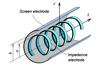
Figure 1 Helix (impedance electrode) in a metal cylinder (screen electrode).

All components of a slow wave will be taken to be proportional to the wave factor exp.(jωt-jβz), where t is time, ω is the angular frequency, and β is the phase constant along coordinate z (β = ω/vph, where vph is the phase velocity of the wave). Any SWS can be characterized by the slowdown N, defined as the ratio of the velocity of light c to the phase velocity of the wave in the SWS, or, that is the same, as

N=β/k MathType@MTEF@5@5@+= feaagKart1ev2aaatCvAUfeBSjuyZL2yd9gzLbvyNv2CaerbuLwBLn hiov2DGi1BTfMBaeXatLxBI9gBaerbd9wDYLwzYbItLDharqqtubsr 4rNCHbGeaGqiVu0Je9sqqrpepC0xbbL8F4rqqrFfpeea0xe9Lq=Jc9 vqaqpepm0xbba9pwe9Q8fs0=yqaqpepae9pg0FirpepeKkFr0xfr=x fr=xb9adbaqaaeGaciGaaiaabeqaamaabaabaaGcbaqcLbsacaWGob Gaeyypa0JaeqOSdiMaai4laiaadUgaaaa@3BA2@ ,      (1)

Where k is the wave number,

k=ω ε 0 μ 0 MathType@MTEF@5@5@+= feaagKart1ev2aaatCvAUfeBSjuyZL2yd9gzLbvyNv2CaerbuLwBLn hiov2DGi1BTfMBaeXatLxBI9gBaerbd9wDYLwzYbItLDharqqtubsr 4rNCHbGeaGqiVu0Je9sqqrpepC0xbbL8F4rqqrFfpeea0xe9Lq=Jc9 vqaqpepm0xbba9pwe9Q8fs0=yqaqpepae9pg0FirpepeKkFr0xfr=x fr=xb9adbaqaaeGaciGaaiaabeqaamaabaabaaGcbaqcLbsacaWGRb Gaeyypa0JaeqyYdCxcfa4aaOaaaOqaaKqzGeGaeqyTduwcfa4aaSba aKqaGeaajugWaiaaicdaaSqabaqcLbsacqaH8oqBjuaGdaWgaaqcba saaKqzadGaaGimaaWcbeaaaeqaaaaa@4503@ ,      (2)

ω is the angular frequency, and ε0, µ0 are the permittivity and permeability of free space.

The impedance electrode is assumed to be a periodic structure in z direction, with period T. When T is small compared with the wavelength (βT<<1), the impedance electrode can be replaced by an anisotropic surface with conductivity in the direction of the winds. This so called impedance approximation significantly simplifies analysis and allows using the equivalent line method. Unlike in waveguides, the phase constant β in slow wave structures always exceeds the wave number; in other words, N>1. In the simplest cases, when the wave front is perpendicular to the wave propagation direction, the electromagnetic field in the transverse cross section is symmetric and depends only on the transverse coordinate, e.g. radius r in axially symmetric structures. The transverse constant γ characterizing this dependence is related to the phase constant and the wave number as

γ 2 = β 2 k 2 MathType@MTEF@5@5@+= feaagKart1ev2aaatCvAUfeBSjuyZL2yd9gzLbvyNv2CaerbuLwBLn hiov2DGi1BTfMBaeXatLxBI9gBaerbd9wDYLwzYbItLDharqqtubsr 4rNCHbGeaGqiVu0Je9sqqrpepC0xbbL8F4rqqrFfpeea0xe9Lq=Jc9 vqaqpepm0xbba9pwe9Q8fs0=yqaqpepae9pg0FirpepeKkFr0xfr=x fr=xb9adbaqaaeGaciGaaiaabeqaamaabaabaaGcbaqcLbsacqaHZo WzjuaGdaahaaWcbeqcbasaaKqzadGaaGOmaaaajugibiabg2da9iab ek7aILqbaoaaCaaaleqajeaibaqcLbmacaaIYaaaaKqzGeGaeyOeI0 Iaam4AaKqbaoaaCaaaleqajeaibaqcLbmacaaIYaaaaaaa@463B@ .      (3)

Unlike the E- and H-waves in waveguides, which exist independently and may be characterized by different equivalent lines,16 slow waves in most SWSs are hybrid waves with components of both E- and H-waves. Having the same phase and group velocities, these waves satisfy different boundary conditions and their transverse distribution can be quite different.

Potential delay

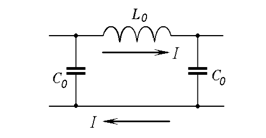
In the impedance approximation, any SWS may be replaced by a two-wire transmission line (Figure 2) with series inductance per unit length L0 and shunt capacitance per unit length C0, in terms of which the phase constant is given by

β 2 = ω 2 L 0 C 0 MathType@MTEF@5@5@+= feaagKart1ev2aaatCvAUfeBSjuyZL2yd9gzLbvyNv2CaerbuLwBLn hiov2DGi1BTfMBaeXatLxBI9gBaerbd9wDYLwzYbItLDharqqtubsr 4rNCHbGeaGqiVu0Je9sqqrpepC0xbbL8F4rqqrFfpeea0xe9Lq=Jc9 vqaqpepm0xbba9pwe9Q8fs0=yqaqpepae9pg0FirpepeKkFr0xfr=x fr=xb9adbaqaaeGaciGaaiaabeqaamaabaabaaGcbaqcLbsacqaHYo GyjuaGdaahaaWcbeqcbasaaKqzadGaaGOmaaaajugibiabg2da9iab eM8a3LqbaoaaCaaaleqajeaibaqcLbmacaaIYaaaaKqzGeGaamitaK qbaoaaBaaajeaibaqcLbmacaaIWaaaleqaaKqzGeGaam4qaKqbaoaa BaaajeaibaqcLbmacaaIWaaaleqaaaaa@4975@ .      (4)

Figure 2 Two-wire equivalent line.

It follows from the rigorous electro-dynamic analysis,17 in the case of slow waves, the dominant part of L0, which we'll designate as L, is defined by the specific inductance of the impedance electrode, while a relatively small part, LD, is defined by the potential delay

L 0 =L+ L D MathType@MTEF@5@5@+= feaagKart1ev2aaatCvAUfeBSjuyZL2yd9gzLbvyNv2CaerbuLwBLn hiov2DGi1BTfMBaeXatLxBI9gBaerbd9wDYLwzYbItLDharqqtubsr 4rNCHbGeaGqiVu0Je9sqqrpepC0xbbL8F4rqqrFfpeea0xe9Lq=Jc9 vqaqpepm0xbba9pwe9Q8fs0=yqaqpepae9pg0FirpepeKkFr0xfr=x fr=xb9adbaqaaeGaciGaaiaabeqaamaabaabaaGcbaqcLbsacaWGmb qcfa4aaSbaaKqaGeaajugWaiaaicdaaSqabaqcLbsacqGH9aqpcaWG mbGaey4kaSIaamitaKqbaoaaBaaajeaibaqcLbmacaWGebaaleqaaa aa@4116@ .       (5)

We emphasize that L depends on the magnetic flow excited by transverse currents, while LD depends on magnetic flow excited by longitudinal currents. In the case of a hybrid wave, L is defined by the H-wave, whereas LD is defined by the E-wave.

Substituting (5) in (4) and comparing with (3), we can identify

ω 2 L D C 0 k 2 MathType@MTEF@5@5@+= feaagKart1ev2aaatCvAUfeBSjuyZL2yd9gzLbvyNv2CaerbuLwBLn hiov2DGi1BTfMBaeXatLxBI9gBaerbd9wDYLwzYbItLDharqqtubsr 4rNCHbGeaGqiVu0Je9sqqrpepC0xbbL8F4rqqrFfpeea0xe9Lq=Jc9 vqaqpepm0xbba9pwe9Q8fs0=yqaqpepae9pg0FirpepeKkFr0xfr=x fr=xb9adbaqaaeGaciGaaiaabeqaamaabaabaaGcbaqcLbsacqaHjp WDjuaGdaahaaWcbeqcbasaaKqzadGaaGOmaaaajugibiaadYeajuaG daWgaaqcbasaaKqzadGaamiraaWcbeaajugibiaadoeajuaGdaWgaa qcbasaaKqzadGaaGimaaWcbeaajugibiabggMi6kaadUgajuaGdaah aaWcbeqcbasaaKqzadGaaGOmaaaaaaa@4996@       (6)

and

γ 2 = ω 2 L C 0 MathType@MTEF@5@5@+= feaagKart1ev2aaatCvAUfeBSjuyZL2yd9gzLbvyNv2CaerbuLwBLn hiov2DGi1BTfMBaeXatLxBI9gBaerbd9wDYLwzYbItLDharqqtubsr 4rNCHbGeaGqiVu0Je9sqqrpepC0xbbL8F4rqqrFfpeea0xe9Lq=Jc9 vqaqpepm0xbba9pwe9Q8fs0=yqaqpepae9pg0FirpepeKkFr0xfr=x fr=xb9adbaqaaeGaciGaaiaabeqaamaabaabaaGcbaqcLbsacqaHZo WzjuaGdaahaaWcbeqcbasaaKqzadGaaGOmaaaajugibiabg2da9iab eM8a3LqbaoaaCaaaleqajeaibaqcLbmacaaIYaaaaKqzGeGaamitai aadoeajuaGdaWgaaqcbasaaKqzadGaaGimaaWcbeaaaaa@4620@ .      (7)

The replacement of L0 by L and traditional long line equation (4) by (7) makes it possible to use circuit theory for all SWSs.

Three-wire equivalent line

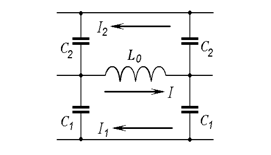
Unlike waveguides, which have only one area with a propagating wave, most SWSs have at least two areas adjacent to opposite surfaces of the impedance electrode. In some cases, for example when one area is filled by a dielectric material or electron beam, it is more convenient to use two shunt capacitances C1 and C2, which relate to the areas adjacent to the impedance electrode from opposite sides. Such a SWS may be represented by a three-wire equivalent line with series inductance in the middle wire and shunt capacitances C1 and C2 connecting the middle wire with lower and upper wires, respectively (Figure 3). The use of electro-dynamic admittances of electric, Ye, and magnetic, Ym, types18 significantly simplifies calculation of the specific parameters of the three-wire equivalent line. As shown in,19 the equivalent capacitance C1 for the area below the impedance electrode, can be defined by the electric type admittance at the bottom surface of the impedance electrode,

C 1 = 2πa γ 2 jω Y 1 e (a) MathType@MTEF@5@5@+= feaagKart1ev2aaatCvAUfeBSjuyZL2yd9gzLbvyNv2CaerbuLwBLn hiov2DGi1BTfMBaeXatLxBI9gBaerbd9wDYLwzYbItLDharqqtubsr 4rNCHbGeaGqiVu0Je9sqqrpepC0xbbL8F4rqqrFfpeea0xe9Lq=Jc9 vqaqpepm0xbba9pwe9Q8fs0=yqaqpepae9pg0FirpepeKkFr0xfr=x fr=xb9adbaqaaeGaciGaaiaabeqaamaabaabaaGcbaqcLbsacaWGdb qcfa4aaSbaaKqaGeaajugWaiaaigdaaSqabaqcLbsacqGH9aqpcqGH sisljuaGdaWcaaGcbaqcLbsacaaIYaGaeqiWdaNaamyyaiabeo7aNL qbaoaaCaaaleqajeaibaqcLbmacaaIYaaaaaGcbaqcLbsacaWGQbGa eqyYdChaaiaadMfajuaGdaqhaaqcbasaaKqzadGaaGymaaqcbasaaK qzadGaamyzaaaajugibiaacIcacaWGHbGaaiykaaaa@51AE@ ,      (8)

Figure 3 Three-wire equivalent line with specific inductance including the potential delay.

Whereas capacitance C2, related to the external (second) area, is

C 2 = 2πa γ 2 jω Y 2 e (a) MathType@MTEF@5@5@+= feaagKart1ev2aaatCvAUfeBSjuyZL2yd9gzLbvyNv2CaerbuLwBLn hiov2DGi1BTfMBaeXatLxBI9gBaerbd9wDYLwzYbItLDharqqtubsr 4rNCHbGeaGqiVu0Je9sqqrpepC0xbbL8F4rqqrFfpeea0xe9Lq=Jc9 vqaqpepm0xbba9pwe9Q8fs0=yqaqpepae9pg0FirpepeKkFr0xfr=x fr=xb9adbaqaaeGaciGaaiaabeqaamaabaabaaGcbaqcLbsacaWGdb qcfa4aaSbaaKqaGeaajugWaiaaikdaaSqabaqcLbsacqGH9aqpjuaG daWcaaGcbaqcLbsacaaIYaGaeqiWdaNaamyyaiabeo7aNLqbaoaaCa aaleqajeaibaqcLbmacaaIYaaaaaGcbaqcLbsacaWGQbGaeqyYdCha aiaadMfajuaGdaqhaaqcbasaaKqzadGaaGOmaaqcbasaaKqzadGaam yzaaaajugibiaacIcacaWGHbGaaiykaaaa@50C3@ ,      (9)

Where in the considered case, a is the impedance electrode's radius. Here and further after, subscripts 1 and 2 are used to denote the internal and external areas, respectively. In the case of a planar electrode, the quantity 2πα in (8) and (9) should be replaced by the electrode’s width, whereas admittances in both cases should be taken on the impedance electrode surfaces. Although L can be split in two parallel inductances related to the different areas, in most cases it is more convenient to use one inductance defined by the jump of the magnetic-type admittances at the impedance electrode

L= 2πa jω h 2 [ Y 2 m (a) Y 1 m (a)] MathType@MTEF@5@5@+= feaagKart1ev2aaatCvAUfeBSjuyZL2yd9gzLbvyNv2CaerbuLwBLn hiov2DGi1BTfMBaeXatLxBI9gBaerbd9wDYLwzYbItLDharqqtubsr 4rNCHbGeaGqiVu0Je9sqqrpepC0xbbL8F4rqqrFfpeea0xe9Lq=Jc9 vqaqpepm0xbba9pwe9Q8fs0=yqaqpepae9pg0FirpepeKkFr0xfr=x fr=xb9adbaqaaeGaciGaaiaabeqaamaabaabaaGcbaqcLbsacaWGmb Gaeyypa0tcfa4aaSaaaOqaaKqzGeGaaGOmaiabec8aWjaadggaaOqa aKqzGeGaamOAaiabeM8a3jaadIgajuaGdaahaaWcbeqcbasaaKqzad GaaGOmaaaajugibiaacUfacaWGzbqcfa4aa0baaKqaGeaajugWaiaa ikdaaKqaGeaajugWaiaad2gaaaqcLbsacaGGOaGaamyyaiaacMcacq GHsislcaWGzbqcfa4aa0baaKqaGeaajugWaiaaigdaaKqaGeaajugW aiaad2gaaaqcLbsacaGGOaGaamyyaiaacMcacaGGDbaaaaaa@58B2@       (10)

According to definition,18

Y 1,2 e (a)= H ϕ1,2 (a) E z1,2 (a) MathType@MTEF@5@5@+= feaagKart1ev2aaatCvAUfeBSjuyZL2yd9gzLbvyNv2CaerbuLwBLn hiov2DGi1BTfMBaeXatLxBI9gBaerbd9wDYLwzYbItLDharqqtubsr 4rNCHbGeaGqiVu0Je9sqqrpepC0xbbL8F4rqqrFfpeea0xe9Lq=Jc9 vqaqpepm0xbba9pwe9Q8fs0=yqaqpepae9pg0FirpepeKkFr0xfr=x fr=xb9adbaqaaeGaciGaaiaabeqaamaabaabaaGcbaqcLbsacaWGzb qcfa4aa0baaKqaGeaajugWaiaaigdacaGGSaGaaGOmaaqcbasaaKqz adGaamyzaaaajugibiaacIcacaWGHbGaaiykaiabg2da9iabgkHiTK qbaoaalaaakeaajugibiaadIeajuaGdaWgaaqcbasaaKqzadGaeqy1 dyMaaGymaiaacYcacaaIYaaaleqaaKqzGeGaaiikaiaadggacaGGPa aakeaajugibiaadweajuaGdaWgaaqcbasaaKqzadGaamOEaiaaigda caGGSaGaaGOmaaWcbeaajugibiaacIcacaWGHbGaaiykaaaaaaa@56D1@ ,      (11)

Y 1,2 m (a)= H z1,2 (a) E ϕ1,2 (a) MathType@MTEF@5@5@+= feaagKart1ev2aaatCvAUfeBSjuyZL2yd9gzLbvyNv2CaerbuLwBLn hiov2DGi1BTfMBaeXatLxBI9gBaerbd9wDYLwzYbItLDharqqtubsr 4rNCHbGeaGqiVu0Je9sqqrpepC0xbbL8F4rqqrFfpeea0xe9Lq=Jc9 vqaqpepm0xbba9pwe9Q8fs0=yqaqpepae9pg0FirpepeKkFr0xfr=x fr=xb9adbaqaaeGaciGaaiaabeqaamaabaabaaGcbaqcLbsacaWGzb qcfa4aa0baaKqaGeaajugWaiaaigdacaGGSaGaaGOmaaqcbasaaKqz adGaamyBaaaajugibiaacIcacaWGHbGaaiykaiabg2da9Kqbaoaala aakeaajugibiaadIeajuaGdaWgaaqcbasaaKqzadGaamOEaiaaigda caGGSaGaaGOmaaWcbeaajugibiaacIcacaWGHbGaaiykaaGcbaqcLb sacaWGfbqcfa4aaSbaaKqaGeaajugWaiabew9aMjaaigdacaGGSaGa aGOmaaWcbeaajugibiaacIcacaWGHbGaaiykaaaaaaa@55EC@ .      (12)

For a planar impedance electrode, transverse coordinates r and ϕ should be replaced by x and y, respectively. Substituting (8)-(10) into (7), one can obtain the lossless version of the general dispersion equation derived in 18 for the helix with losses

(2πa) 2 Δ Y e h 2 Δ Y m +1=0 MathType@MTEF@5@5@+= feaagKart1ev2aaatCvAUfeBSjuyZL2yd9gzLbvyNv2CaerbuLwBLn hiov2DGi1BTfMBaeXatLxBI9gBaerbd9wDYLwzYbItLDharqqtubsr 4rNCHbGeaGqiVu0Je9sqqrpepC0xbbL8F4rqqrFfpeea0xe9Lq=Jc9 vqaqpepm0xbba9pwe9Q8fs0=yqaqpepae9pg0FirpepeKkFr0xfr=x fr=xb9adbaqaaeGaciGaaiaabeqaamaabaabaaGcbaqcfa4aaSaaaO qaaKqzGeGaaiikaiaaikdacqaHapaCcaWGHbGaaiykaKqbaoaaCaaa leqajeaibaqcLbmacaaIYaaaaKqzGeGaeuiLdqKaamywaKqbaoaaCa aaleqajeaibaqcLbmacaWGLbaaaaGcbaqcLbsacaWGObqcfa4aaWba aSqabKqaGeaajugWaiaaikdaaaqcLbsacqqHuoarcaWGzbqcfa4aaW baaSqabKqaGeaajugWaiaad2gaaaaaaKqzGeGaey4kaSIaaGymaiab g2da9iaaicdaaaa@529D@ .      (13)

Transition from a three-wire to a two-wire equivalent line is possible by adding together shunt capacitances, taking into account the difference in potential delays in the areas with different permittivity,19

C 0 = C 1 + γ 1 2 C 2 / γ 2 2 MathType@MTEF@5@5@+= feaagKart1ev2aaatCvAUfeBSjuyZL2yd9gzLbvyNv2CaerbuLwBLn hiov2DGi1BTfMBaeXatLxBI9gBaerbd9wDYLwzYbItLDharqqtubsr 4rNCHbGeaGqiVu0Je9sqqrpepC0xbbL8F4rqqrFfpeea0xe9Lq=Jc9 vqaqpepm0xbba9pwe9Q8fs0=yqaqpepae9pg0FirpepeKkFr0xfr=x fr=xb9adbaqaaeGaciGaaiaabeqaamaabaabaaGcbaqcLbsacaWGdb qcfa4aaSbaaKqaGeaajugWaiaaicdaaSqabaqcLbsacqGH9aqpcaWG dbqcfa4aaSbaaKqaGeaajugWaiaaigdaaSqabaqcLbsacqGHRaWkcq aHZoWzjuaGdaqhaaqcbasaaKqzadGaaGymaaqcbasaaKqzadGaaGOm aaaajugibiaadoeajuaGdaWgaaqcbasaaKqzadGaaGOmaaWcbeaaju gibiaac+cacqaHZoWzjuaGdaqhaaqcbasaaKqzadGaaGOmaaqcbasa aKqzadGaaGOmaaaaaaa@5318@ ,      (14)

Where

γ 1,2 2 = β 2 k 2 ε 1,2 MathType@MTEF@5@5@+= feaagKart1ev2aaatCvAUfeBSjuyZL2yd9gzLbvyNv2CaerbuLwBLn hiov2DGi1BTfMBaeXatLxBI9gBaerbd9wDYLwzYbItLDharqqtubsr 4rNCHbGeaGqiVu0Je9sqqrpepC0xbbL8F4rqqrFfpeea0xe9Lq=Jc9 vqaqpepm0xbba9pwe9Q8fs0=yqaqpepae9pg0FirpepeKkFr0xfr=x fr=xb9adbaqaaeGaciGaaiaabeqaamaabaabaaGcbaqcLbsacqaHZo WzjuaGdaqhaaqcbasaaKqzadGaaGymaiaacYcacaaIYaaajeaibaqc LbmacaaIYaaaaKqzGeGaeyypa0JaeqOSdiwcfa4aaWbaaSqabKqaGe aajugWaiaaikdaaaqcLbsacqGHsislcaWGRbqcfa4aaWbaaSqabKqa GeaajugWaiaaikdaaaqcLbsacqaH1oqzjuaGdaWgaaqcbasaaKqzad GaaGymaiaacYcacaaIYaaaleqaaaaa@501E@ ,      (15)

and subscripts refer to different areas with relative permittivities ε1ανδε 2

Effective voltage

The peculiarity of all dispersive transmission lines is in the longitudinal capacitive (displacement) currents, which unlike the conduction currents in the electrodes, are subjected to smaller voltages than the voltage U between electrodes. This leads to a decrease in the power flow P as compared to the quantity UI/2. The conduction current passing through the screen electrode is only a part of the current in the impedance electrode, the rest being the longitudinal capacitive current. Equality of current amplitudes in the two-wire equivalent line is due to summing these currents. As a result, replacing transmission structures with longitudinal capacitive currents by equivalent lines leads to an incorrect definition of the power flow and, consequently, the wave impedance. Although the product L0C0, determined by formulas (8)-(10) gives correct dispersion equations, the ratio L0/C0 determining the wave impedance, is incorrect. As it was shown in,16 this problem may be solved by (1) introducing an effective voltage Uef, (2) reducing the equivalent inductance, and (3) increasing the equivalent capacitances. Voltage U at the impedance electrode and current I as well as the real power flow P may be found with help of expressions for components of the slow wave, obtained from solutions of the wave equations in the areas adjacent to the impedance electrode. For the same current and power flow in the equivalent line,

U ef =2P/| I | MathType@MTEF@5@5@+= feaagKart1ev2aaatCvAUfeBSjuyZL2yd9gzLbvyNv2CaerbuLwBLn hiov2DGi1BTfMBaeXatLxBI9gBaerbd9wDYLwzYbItLDharqqtubsr 4rNCHbGeaGqiVu0Je9sqqrpepC0xbbL8F4rqqrFfpeea0xe9Lq=Jc9 vqaqpepm0xbba9pwe9Q8fs0=yqaqpepae9pg0FirpepeKkFr0xfr=x fr=xb9adbaqaaeGaciGaaiaabeqaamaabaabaaGcbaqcLbsacaWGvb WcdaWgaaqcbasaaKqzadGaamyzaiaadAgaaKqaGeqaaKqzGeGaeyyp a0JaaGOmaiaadcfacaGGVaqcfa4aaqWaaOqaaKqzGeGaamysaaGcca GLhWUaayjcSdaaaa@43DC@ ,      (16)

Where | I | MathType@MTEF@5@5@+= feaagKart1ev2aaatCvAUfeBSjuyZL2yd9gzLbvyNv2CaerbuLwBLn hiov2DGi1BTfMBaeXatLxBI9gBaerbd9wDYLwzYbItLDharqqtubsr 4rNCHbGeaGqiVu0Je9sqqrpepC0xbbL8F4rqqrFfpeea0xe9Lq=Jc9 vqaqpepm0xbba9pwe9Q8fs0=yqaqpepae9pg0FirpepeKkFr0xfr=x fr=xb9adbaqaaeGaciGaaiaabeqaamaabaabaaGcbaqcfa4aaqWaaO qaaKqzGeGaamysaaGccaGLhWUaayjcSdaaaa@3B17@ is the amplitude of the conduction current in the impedance electrode. We define the voltage correction coefficient U ef /U MathType@MTEF@5@5@+= feaagKart1ev2aaatCvAUfeBSjuyZL2yd9gzLbvyNv2CaerbuLwBLn hiov2DGi1BTfMBaeXatLxBI9gBaerbd9wDYLwzYbItLDharqqtubsr 4rNCHbGeaGqiVu0Je9sqqrpepC0xbbL8F4rqqrFfpeea0xe9Lq=Jc9 vqaqpepm0xbba9pwe9Q8fs0=yqaqpepae9pg0FirpepeKkFr0xfr=x fr=xb9adbaqaaeGaciGaaiaabeqaamaabaabaaGcbaqcLbsacaWGvb qcfa4aaSbaaKqaGeaajugWaiaadwgacaWGMbaaleqaaKqzGeGaai4l aiaadwfaaaa@3D62@  as

ψ U ef /U MathType@MTEF@5@5@+= feaagKart1ev2aaatCvAUfeBSjuyZL2yd9gzLbvyNv2CaerbuLwBLn hiov2DGi1BTfMBaeXatLxBI9gBaerbd9wDYLwzYbItLDharqqtubsr 4rNCHbGeaGqiVu0Je9sqqrpepC0xbbL8F4rqqrFfpeea0xe9Lq=Jc9 vqaqpepm0xbba9pwe9Q8fs0=yqaqpepae9pg0FirpepeKkFr0xfr=x fr=xb9adbaqaaeGaciGaaiaabeqaamaabaabaaGcbaqcLbsacqaHip qEcqGHHjIUcaWGvbqcfa4aaSbaaKazba4=baqcLbmacaWGLbGaamOz aaqcbawabaqcLbsacaGGVaGaamyvaaaa@431B@ .      (17)

The correction coefficient y is always less than 1. The decrease in Uef should be followed by a proportional decrease in L0 and L and the proportional increase in the shunt capacitance or capacitances. In the case of a two-wire truncated equivalent line, the equivalent series inductance and shunt capacitance are therefore:

L ef =ψL , C ef = C 0 /ψ MathType@MTEF@5@5@+= feaagKart1ev2aaatCvAUfeBSjuyZL2yd9gzLbvyNv2CaerbuLwBLn hiov2DGi1BTfMBaeXatLxBI9gBaerbd9wDYLwzYbItLDharqqtubsr 4rNCHbGeaGqiVu0Je9sqqrpepC0xbbL8F4rqqrFfpeea0xe9Lq=Jc9 vqaqpepm0xbba9pwe9Q8fs0=yqaqpepae9pg0FirpepeKkFr0xfr=x fr=xb9adbaqaaeGaciGaaiaabeqaamaabaabaaGcbaqcLbsacaWGmb qcfa4aaSbaaKqaGeaajugWaiaadwgacaWGMbaaleqaaKqzGeGaeyyp a0JaeqiYdKNaamitaiaacYcalmaaDaaajeaibaaabaaaaKqzGeGaam 4qaKqbaoaaBaaajeaibaqcLbmacaWGLbGaamOzaaWcbeaajugibiab g2da9iaadoeajuaGdaWgaaqcbasaaKqzadGaaGimaaWcbeaajugibi aac+cacqaHipqEaaa@4DEF@ ,      (18)

It is seen that substitution of (17) and (18) in (7) does not change the dispersion equation, while the wave impedance can be defined unambiguously

Z 0 = U ef I 2P I 2 U ef 2 2P β γ L ef C ef MathType@MTEF@5@5@+= feaagKart1ev2aaatCvAUfeBSjuyZL2yd9gzLbvyNv2CaerbuLwBLn hiov2DGi1BTfMBaeXatLxBI9gBaerbd9wDYLwzYbItLDharqqtubsr 4rNCHbGeaGqiVu0Je9sqqrpepC0xbbL8F4rqqrFfpeea0xe9Lq=Jc9 vqaqpepm0xbba9pwe9Q8fs0=yqaqpepae9pg0FirpepeKkFr0xfr=x fr=xb9adbaqaaeGaciGaaiaabeqaamaabaabaaGcbaqcLbsacaWGAb qcfa4aaSbaaKqaGeaajugWaiaaicdaaSqabaqcLbsacqGH9aqpjuaG daWcaaGcbaqcLbsacaWGvbqcfa4aaSbaaKqaGeaajugWaiaadwgaca WGMbaaleqaaaGcbaqcLbsacaWGjbaaaiabggMi6Mqbaoaalaaakeaa jugibiaaikdacaWGqbaakeaajugibiaadMeajuaGdaahaaWcbeqcba saaKqzadGaaGOmaaaaaaqcLbsacqGHHjIUjuaGdaWcaaGcbaqcLbsa caWGvbqcfa4aa0baaKqaGeaajugWaiaadwgacaWGMbaajeaibaqcLb macaaIYaaaaaGcbaqcLbsacaaIYaGaamiuaaaacqGHHjIUjuaGdaWc aaGcbaqcLbsacqaHYoGyaOqaaKqzGeGaeq4SdCgaaKqbaoaakaaake aajuaGdaWcaaGcbaqcLbsacaWGmbqcfa4aaSbaaKqaGeaajugWaiaa dwgacaWGMbaaleqaaaGcbaqcLbsacaWGdbqcfa4aaSbaaKqaGeaaju gWaiaadwgacaWGMbaaleqaaaaaaeqaaaaa@6B2F@ .      (19)

In the following section we demonstrate the application of these relations to the sheath helix in free space.

Free helix

The helix is the most frequently used and analyzed SWS. Even so, the published expressions for specific inductance and capacitance satisfying the transmission line dispersion equation do not satisfy the formulas for the wave impedance. Although in practice, the helix is used with a screen electrode; its diameter is chosen large enough to minimize its influence on the field in the helix. For the sake of simplicity we restrict our analysis to a helix in the absence of the screen electrode (free helix). The following formulas for specific inductance and capacitance and for power flow for the free helix had been derived previously:1,6,7,18

L= μ 0 tan 2 Φ 2π I 1 (γa) K 1 (γa) MathType@MTEF@5@5@+= feaagKart1ev2aaatCvAUfeBSjuyZL2yd9gzLbvyNv2CaerbuLwBLn hiov2DGi1BTfMBaeXatLxBI9gBaerbd9wDYLwzYbItLDharqqtubsr 4rNCHbGeaGqiVu0Je9sqqrpepC0xbbL8F4rqqrFfpeea0xe9Lq=Jc9 vqaqpepm0xbba9pwe9Q8fs0=yqaqpepae9pg0FirpepeKkFr0xfr=x fr=xb9adbaqaaeGaciGaaiaabeqaamaabaabaaGcbaqcLbsacaWGmb Gaeyypa0JaeqiVd0wcfa4aaSbaaKqaGeaajugWaiaaicdaaSqabaqc fa4aaSaaaOqaaKqzGeGaciiDaiaacggacaGGUbqcfa4aaWbaaSqabK qaGeaajugWaiaaikdaaaqcLbsacqqHMoGraOqaaKqzGeGaaGOmaiab ec8aWbaacaWGjbqcfa4aaSbaaKqaGeaajugWaiaaigdaaSqabaqcLb sacaGGOaGaeq4SdCMaamyyaiaacMcacaWGlbqcfa4aaSbaaKqaGeaa jugWaiaaigdaaSqabaqcLbsacaGGOaGaeq4SdCMaamyyaiaacMcaaa a@58F2@ ,      (20)

C 0 = ε 0 2π I 0 (γa) K 0 (γa) MathType@MTEF@5@5@+= feaagKart1ev2aaatCvAUfeBSjuyZL2yd9gzLbvyNv2CaerbuLwBLn hiov2DGi1BTfMBaeXatLxBI9gBaerbd9wDYLwzYbItLDharqqtubsr 4rNCHbGeaGqiVu0Je9sqqrpepC0xbbL8F4rqqrFfpeea0xe9Lq=Jc9 vqaqpepm0xbba9pwe9Q8fs0=yqaqpepae9pg0FirpepeKkFr0xfr=x fr=xb9adbaqaaeGaciGaaiaabeqaamaabaabaaGcbaqcLbsacaWGdb qcfa4aaSbaaKqaGeaajugWaiaaicdaaSqabaqcLbsacqGH9aqpjuaG daWcaaGcbaqcLbsacqaH1oqzjuaGdaWgaaqcbasaaKqzadGaaGimaa WcbeaajugibiaaikdacqaHapaCaOqaaKqzGeGaamysaKqbaoaaBaaa jeaibaqcLbmacaaIWaaaleqaaKqzGeGaaiikaiabeo7aNjaadggaca GGPaGaam4saKqbaoaaBaaajeaibaqcLbmacaaIWaaaleqaaKqzGeGa aiikaiabeo7aNjaadggacaGGPaaaaaaa@5519@ ,      (21)

P= ω ε 0 πβa A 2 2 γ 3 I 0 (γa) K 0 (γa) F(γa) MathType@MTEF@5@5@+= feaagKart1ev2aaatCvAUfeBSjuyZL2yd9gzLbvyNv2CaerbuLwBLn hiov2DGi1BTfMBaeXatLxBI9gBaerbd9wDYLwzYbItLDharqqtubsr 4rNCHbGeaGqiVu0Je9sqqrpepC0xbbL8F4rqqrFfpeea0xe9Lq=Jc9 vqaqpepm0xbba9pwe9Q8fs0=yqaqpepae9pg0FirpepeKkFr0xfr=x fr=xb9adbaqaaeGaciGaaiaabeqaamaabaabaaGcbaqcLbsacaWGqb Gaeyypa0tcfa4aaSaaaOqaaKqzGeGaeqyYdCNaeqyTduwcfa4aaSba aKqaGeaajugWaiaaicdaaSqabaqcLbsacqaHapaCcqaHYoGycaWGHb GaamyqaKqbaoaaCaaaleqajeaibaqcLbmacaaIYaaaaaGcbaqcLbsa caaIYaGaeq4SdCwcfa4aaWbaaSqabKqaGeaajugWaiaaiodaaaaaaK qbaoaalaaakeaajugibiaadMeajuaGdaWgaaqcbasaaKqzadGaaGim aaWcbeaajugibiaacIcacqaHZoWzcaWGHbGaaiykaaGcbaqcLbsaca WGlbqcfa4aaSbaaKqaGeaajugWaiaaicdaaSqabaqcLbsacaGGOaGa eq4SdCMaamyyaiaacMcaaaGaamOraiaacIcacqaHZoWzcaWGHbGaai ykaaaa@64AC@       (22)

where I0,1 and K0,1 are the modified Bessel functions of the first and second kinds, zero and first orders, Φ is the angle between the direction of the helix conductivity and longitudinal axis, F(x) is an auxiliary function

F(x)= 4 x + I 1 (x) I 0 (x) I 0 (x) I 1 (x) + K 0 (x) K 1 (x) K 1 (x) K 0 (x) MathType@MTEF@5@5@+= feaagKart1ev2aaatCvAUfeBSjuyZL2yd9gzLbvyNv2CaerbuLwBLn hiov2DGi1BTfMBaeXatLxBI9gBaerbd9wDYLwzYbItLDharqqtubsr 4rNCHbGeaGqiVu0Je9sqqrpepC0xbbL8F4rqqrFfpeea0xe9Lq=Jc9 vqaqpepm0xbba9pwe9Q8fs0=yqaqpepae9pg0FirpepeKkFr0xfr=x fr=xb9adbaqaaeGaciGaaiaabeqaamaabaabaaGcbaqcLbsacaWGgb GaaiikaiaadIhacaGGPaGaeyypa0tcfa4aaSaaaOqaaKqzGeGaaGin aaGcbaqcLbsacaWG4baaaiabgUcaRKqbaoaalaaakeaajugibiaadM eajuaGdaWgaaqcbasaaKqzadGaaGymaaWcbeaajugibiaacIcacaWG 4bGaaiykaaGcbaqcLbsacaWGjbqcfa4aaSbaaKqaGeaajugWaiaaic daaSqabaqcLbsacaGGOaGaamiEaiaacMcaaaGaeyOeI0scfa4aaSaa aOqaaKqzGeGaamysaKqbaoaaBaaajeaibaqcLbmacaaIWaaaleqaaK qzGeGaaiikaiaadIhacaGGPaaakeaajugibiaadMeajuaGdaWgaaqc basaaKqzadGaaGymaaWcbeaajugibiaacIcacaWG4bGaaiykaaaacq GHRaWkjuaGdaWcaaGcbaqcLbsacaWGlbqcfa4aaSbaaKqaGeaajugW aiaaicdaaSqabaqcLbsacaGGOaGaamiEaiaacMcaaOqaaKqzGeGaam 4saKqbaoaaBaaajeaibaqcLbmacaaIXaaaleqaaKqzGeGaaiikaiaa dIhacaGGPaaaaiabgkHiTKqbaoaalaaakeaajugibiaadUeajuaGda WgaaqcbasaaKqzadGaaGymaaWcbeaajugibiaacIcacaWG4bGaaiyk aaGcbaqcLbsacaWGlbqcfa4aaSbaaKqaGeaajugWaiaaicdaaSqaba qcLbsacaGGOaGaamiEaiaacMcaaaaaaa@7D19@ ,       (23)

Whereas A is the constant in the formulas for the longitudinal components of the electric field intensity

E z1 (r)=A I 0 (γr) MathType@MTEF@5@5@+= feaagKart1ev2aaatCvAUfeBSjuyZL2yd9gzLbvyNv2CaerbuLwBLn hiov2DGi1BTfMBaeXatLxBI9gBaerbd9wDYLwzYbItLDharqqtubsr 4rNCHbGeaGqiVu0Je9sqqrpepC0xbbL8F4rqqrFfpeea0xe9Lq=Jc9 vqaqpepm0xbba9pwe9Q8fs0=yqaqpepae9pg0FirpepeKkFr0xfr=x fr=xb9adbaqaaeGaciGaaiaabeqaamaabaabaaGcbaqcLbsacaWGfb qcfa4aaSbaaKqaGeaajugWaiaadQhacaaIXaaaleqaaKqzGeGaaiik aiaadkhacaGGPaGaeyypa0JaamyqaiaadMeajuaGdaWgaaqcbasaaK qzadGaaGimaaWcbeaajugibiaacIcacqaHZoWzcaWGYbGaaiykaaaa @47E6@ ,      (24)

E z2 (r)=A I 0 (γa) K 0 (γa) K 0 (γr) MathType@MTEF@5@5@+= feaagKart1ev2aaatCvAUfeBSjuyZL2yd9gzLbvyNv2CaerbuLwBLn hiov2DGi1BTfMBaeXatLxBI9gBaerbd9wDYLwzYbItLDharqqtubsr 4rNCHbGeaGqiVu0Je9sqqrpepC0xbbL8F4rqqrFfpeea0xe9Lq=Jc9 vqaqpepm0xbba9pwe9Q8fs0=yqaqpepae9pg0FirpepeKkFr0xfr=x fr=xb9adbaqaaeGaciGaaiaabeqaamaabaabaaGcbaqcLbsacaWGfb qcfa4aaSbaaKqaGeaajugWaiaadQhacaaIYaaaleqaaKqzGeGaaiik aiaadkhacaGGPaGaeyypa0JaamyqaKqbaoaalaaakeaajugibiaadM eajuaGdaWgaaqcbasaaKqzadGaaGimaaWcbeaajugibiaacIcacqaH ZoWzcaWGHbGaaiykaaGcbaqcLbsacaWGlbqcfa4aaSbaaKqaGeaaju gWaiaaicdaaSqabaqcLbsacaGGOaGaeq4SdCMaamyyaiaacMcaaaGa am4saKqbaoaaBaaajeaibaqcLbmacaaIWaaaleqaaKqzGeGaaiikai abeo7aNjaadkhacaGGPaaaaa@59D9@ .      (25)

The dispersion equation for the free helix can be found by substituting (20) and (21) in (7):

γ 2 k 2 = I 1 (γa) K 1 (γa) I 0 (γa) K 0 (γa) tan 2 Φ MathType@MTEF@5@5@+= feaagKart1ev2aaatCvAUfeBSjuyZL2yd9gzLbvyNv2CaerbuLwBLn hiov2DGi1BTfMBaeXatLxBI9gBaerbd9wDYLwzYbItLDharqqtubsr 4rNCHbGeaGqiVu0Je9sqqrpepC0xbbL8F4rqqrFfpeea0xe9Lq=Jc9 vqaqpepm0xbba9pwe9Q8fs0=yqaqpepae9pg0FirpepeKkFr0xfr=x fr=xb9adbaqaaeGaciGaaiaabeqaamaabaabaaGcbaqcfa4aaSaaaO qaaKqzGeGaeq4SdCwcfa4aaWbaaSqabKqaGeaajugWaiaaikdaaaaa keaajugibiaadUgajuaGdaahaaWcbeqcbasaaKqzadGaaGOmaaaaaa qcLbsacqGH9aqpjuaGdaWcaaGcbaqcLbsacaWGjbqcfa4aaSbaaKqa GeaajugWaiaaigdaaSqabaqcLbsacaGGOaGaeq4SdCMaamyyaiaacM cacaWGlbqcfa4aaSbaaKqaGeaajugWaiaaigdaaSqabaqcLbsacaGG OaGaeq4SdCMaamyyaiaacMcaaOqaaKqzGeGaamysaKqbaoaaBaaaje aibaqcLbmacaaIWaaaleqaaKqzGeGaaiikaiabeo7aNjaadggacaGG PaGaam4saKqbaoaaBaaajeaibaqcLbmacaaIWaaaleqaaKqzGeGaai ikaiabeo7aNjaadggacaGGPaaaaiGacshacaGGHbGaaiOBaKqbaoaa CaaaleqajeaibaqcLbmacaaIYaaaaKqzGeGaeuOPdyeaaa@6B4B@ .      (26)

Equating the conduction current density to the jump of the azimuth components of the magnetic field intensity at the helix and multiplying by 2πα, one obtains the current

I=2πA jω ε 0 γ 2 K 0 (γa) MathType@MTEF@5@5@+= feaagKart1ev2aaatCvAUfeBSjuyZL2yd9gzLbvyNv2CaerbuLwBLn hiov2DGi1BTfMBaeXatLxBI9gBaerbd9wDYLwzYbItLDharqqtubsr 4rNCHbGeaGqiVu0Je9sqqrpepC0xbbL8F4rqqrFfpeea0xe9Lq=Jc9 vqaqpepm0xbba9pwe9Q8fs0=yqaqpepae9pg0FirpepeKkFr0xfr=x fr=xb9adbaqaaeGaciGaaiaabeqaamaabaabaaGcbaqcLbsacaWGjb Gaeyypa0JaeyOeI0IaaGOmaiabec8aWjaadgeajuaGdaWcaaGcbaqc LbsacaWGQbGaeqyYdCNaeqyTduwcfa4aaSbaaKqaGeaajugWaiaaic daaSqabaaakeaajugibiabeo7aNLqbaoaaCaaaleqajeaibaqcLbma caaIYaaaaKqzGeGaam4saKqbaoaaBaaajeaibaqcLbmacaaIWaaale qaaKqzGeGaaiikaiabeo7aNjaadggacaGGPaaaaaaa@529A@ .      (27)

The potential U at the helix can be obtained by integrating Ez2(r) from a to infinity,

U= jβ γ 2 E z (a)= jβ γ 2 A I 0 (γa) MathType@MTEF@5@5@+= feaagKart1ev2aaatCvAUfeBSjuyZL2yd9gzLbvyNv2CaerbuLwBLn hiov2DGi1BTfMBaeXatLxBI9gBaerbd9wDYLwzYbItLDharqqtubsr 4rNCHbGeaGqiVu0Je9sqqrpepC0xbbL8F4rqqrFfpeea0xe9Lq=Jc9 vqaqpepm0xbba9pwe9Q8fs0=yqaqpepae9pg0FirpepeKkFr0xfr=x fr=xb9adbaqaaeGaciGaaiaabeqaamaabaabaaGcbaqcLbsacaWGvb Gaeyypa0JaeyOeI0scfa4aaSaaaOqaaKqzGeGaamOAaiabek7aIbGc baqcLbsacqaHZoWzjuaGdaahaaWcbeqcbasaaKqzadGaaGOmaaaaaa qcLbsacaWGfbqcfa4aaSbaaKqaGeaajugWaiaadQhaaSqabaqcLbsa caGGOaGaamyyaiaacMcacqGH9aqpjuaGdaWcaaGcbaqcLbsacaWGQb GaeqOSdigakeaajugibiabeo7aNLqbaoaaCaaaleqajeaibaqcLbma caaIYaaaaaaajugibiaadgeacaWGjbqcfa4aaSbaaKqaGeaajugWai aaicdaaSqabaqcLbsacaGGOaGaeq4SdCMaamyyaiaacMcaaaa@5CA0@ . (28)

Substituting (22) and (27) into (16) gives the effective voltage

| U ef |= βaA 4γ I 0 (γa)F(γa) MathType@MTEF@5@5@+= feaagKart1ev2aaatCvAUfeBSjuyZL2yd9gzLbvyNv2CaerbuLwBLn hiov2DGi1BTfMBaeXatLxBI9gBaerbd9wDYLwzYbItLDharqqtubsr 4rNCHbGeaGqiVu0Je9sqqrpepC0xbbL8F4rqqrFfpeea0xe9Lq=Jc9 vqaqpepm0xbba9pwe9Q8fs0=yqaqpepae9pg0FirpepeKkFr0xfr=x fr=xb9adbaqaaeGaciGaaiaabeqaamaabaabaaGcbaqcfa4aaqWaaO qaaKqzGeGaamyvaKqbaoaaBaaajeaibaqcLbmacaWGLbGaamOzaaWc beaaaOGaay5bSlaawIa7aKqzGeGaeyypa0tcfa4aaSaaaOqaaKqzGe GaeqOSdiMaamyyaiaadgeaaOqaaKqzGeGaaGinaiabeo7aNbaacaWG jbqcfa4aaSbaaKqaGeaajugWaiaaicdaaSqabaqcLbsacaGGOaGaeq 4SdCMaamyyaiaacMcacaWGgbGaaiikaiabeo7aNjaadggacaGGPaaa aa@54E1@ . (29)

and

ψ=| U ef U |= γa 4 F(γa) MathType@MTEF@5@5@+= feaagKart1ev2aaatCvAUfeBSjuyZL2yd9gzLbvyNv2CaerbuLwBLn hiov2DGi1BTfMBaeXatLxBI9gBaerbd9wDYLwzYbItLDharqqtubsr 4rNCHbGeaGqiVu0Je9sqqrpepC0xbbL8F4rqqrFfpeea0xe9Lq=Jc9 vqaqpepm0xbba9pwe9Q8fs0=yqaqpepae9pg0FirpepeKkFr0xfr=x fr=xb9adbaqaaeGaciGaaiaabeqaamaabaabaaGcbaqcLbsacqaHip qEcqGH9aqpjuaGdaabdaGcbaqcfa4aaSaaaOqaaKqzGeGaamyvaKqb aoaaBaaajeaibaqcLbmacaWGLbGaamOzaaWcbeaaaOqaaKqzGeGaam yvaaaaaOGaay5bSlaawIa7aKqzGeGaeyypa0tcfa4aaSaaaOqaaKqz GeGaeq4SdCMaamyyaaGcbaqcLbsacaaI0aaaaiaadAeacaGGOaGaeq 4SdCMaamyyaiaacMcaaaa@4FE9@ . (30)

It follows from (18), (20), (21), and (30) that for the free helix

L ef = μ 0 tan 2 Φ 8π γa I 1 (γa) K 1 (γa)F(γa) MathType@MTEF@5@5@+= feaagKart1ev2aaatCvAUfeBSjuyZL2yd9gzLbvyNv2CaerbuLwBLn hiov2DGi1BTfMBaeXatLxBI9gBaerbd9wDYLwzYbItLDharqqtubsr 4rNCHbGeaGqiVu0Je9sqqrpepC0xbbL8F4rqqrFfpeea0xe9Lq=Jc9 vqaqpepm0xbba9pwe9Q8fs0=yqaqpepae9pg0FirpepeKkFr0xfr=x fr=xb9adbaqaaeGaciGaaiaabeqaamaabaabaaGcbaqcLbsacaWGmb qcfa4aaSbaaKqaGeaajugWaiaadwgacaWGMbaaleqaaKqzGeGaeyyp a0JaeqiVd0wcfa4aaSbaaKqaGeaajugWaiaaicdaaSqabaqcfa4aaS aaaOqaaKqzGeGaciiDaiaacggacaGGUbqcfa4aaWbaaSqabKqaGeaa jugWaiaaikdaaaqcLbsacqqHMoGraOqaaKqzGeGaaGioaiabec8aWb aacqaHZoWzcaWGHbGaamysaKqbaoaaBaaajeaibaqcLbmacaaIXaaa leqaaKqzGeGaaiikaiabeo7aNjaadggacaGGPaGaam4saKqbaoaaBa aajeaibaqcLbmacaaIXaaaleqaaKqzGeGaaiikaiabeo7aNjaadgga caGGPaGaamOraiaacIcacqaHZoWzcaWGHbGaaiykaaaa@64AC@ , (31)

C ef = ε 0 8π γa I 0 (γa) K 0 (γa)F(γa) MathType@MTEF@5@5@+= feaagKart1ev2aaatCvAUfeBSjuyZL2yd9gzLbvyNv2CaerbuLwBLn hiov2DGi1BTfMBaeXatLxBI9gBaerbd9wDYLwzYbItLDharqqtubsr 4rNCHbGeaGqiVu0Je9sqqrpepC0xbbL8F4rqqrFfpeea0xe9Lq=Jc9 vqaqpepm0xbba9pwe9Q8fs0=yqaqpepae9pg0FirpepeKkFr0xfr=x fr=xb9adbaqaaeGaciGaaiaabeqaamaabaabaaGcbaqcLbsacaWGdb qcfa4aaSbaaKqaGeaajugWaiaadwgacaWGMbaaleqaaKqzGeGaeyyp a0tcfa4aaSaaaOqaaKqzGeGaeqyTduwcfa4aaSbaaKqaGeaajugWai aaicdaaSqabaqcLbsacaaI4aGaeqiWdahakeaajugibiabeo7aNjaa dggacaWGjbqcfa4aaSbaaKqaGeaajugWaiaaicdaaSqabaqcLbsaca GGOaGaeq4SdCMaamyyaiaacMcacaWGlbqcfa4aaSbaaKqaGeaajugW aiaaicdaaSqabaqcLbsacaGGOaGaeq4SdCMaamyyaiaacMcacaWGgb Gaaiikaiabeo7aNjaadggacaGGPaaaaaaa@5D78@ . (32)

Using (31) and (32) in (19) gives the formula for the wave impedance:

Z 0 = μ 0 ε 0 β γ γaF(γa) 8π f(γa)tanΦ MathType@MTEF@5@5@+= feaagKart1ev2aaatCvAUfeBSjuyZL2yd9gzLbvyNv2CaerbuLwBLn hiov2DGi1BTfMBaeXatLxBI9gBaerbd9wDYLwzYbItLDharqqtubsr 4rNCHbGeaGqiVu0Je9sqqrpepC0xbbL8F4rqqrFfpeea0xe9Lq=Jc9 vqaqpepm0xbba9pwe9Q8fs0=yqaqpepae9pg0FirpepeKkFr0xfr=x fr=xb9adbaqaaeGaciGaaiaabeqaamaabaabaaGcbaqcLbsacaWGAb qcfa4aaSbaaKqaGeaajugWaiaaicdaaSqabaqcLbsacqGH9aqpjuaG daGcaaGcbaqcfa4aaSaaaOqaaKqzGeGaeqiVd0wcfa4aaSbaaKqaGe aajugWaiaaicdaaSqabaaakeaajugibiabew7aLLqbaoaaBaaajeai baqcLbmacaaIWaaaleqaaaaaaeqaaKqbaoaalaaakeaajugibiabek 7aIbGcbaqcLbsacqaHZoWzaaqcfa4aaSaaaOqaaKqzGeGaeq4SdCMa amyyaiaadAeacaGGOaGaeq4SdCMaamyyaiaacMcaaOqaaKqzGeGaaG ioaiabec8aWbaacaWGMbGaaiikaiabeo7aNjaadggacaGGPaGaciiD aiaacggacaGGUbGaeuOPdyeaaa@60F3@ , (33)

Where

f(γa)= I 0 (γa) K 0 (γa) I 1 (γa) K 1 (γa) MathType@MTEF@5@5@+= feaagKart1ev2aaatCvAUfeBSjuyZL2yd9gzLbvyNv2CaerbuLwBLn hiov2DGi1BTfMBaeXatLxBI9gBaerbd9wDYLwzYbItLDharqqtubsr 4rNCHbGeaGqiVu0Je9sqqrpepC0xbbL8F4rqqrFfpeea0xe9Lq=Jc9 vqaqpepm0xbba9pwe9Q8fs0=yqaqpepae9pg0FirpepeKkFr0xfr=x fr=xb9adbaqaaeGaciGaaiaabeqaamaabaabaaGcbaqcLbsacaWGMb Gaaiikaiabeo7aNjaadggacaGGPaGaeyypa0tcfa4aaOaaaOqaaKqz GeGaamysaKqbaoaaBaaajeaibaqcLbmacaaIWaaaleqaaKqzGeGaai ikaiabeo7aNjaadggacaGGPaGaam4saKqbaoaaBaaajeaibaqcLbma caaIWaaaleqaaKqzGeGaaiikaiabeo7aNjaadggacaGGPaGaamysaK qbaoaaBaaajeaibaqcLbmacaaIXaaaleqaaKqzGeGaaiikaiabeo7a NjaadggacaGGPaGaam4saKqbaoaaBaaajeaibaqcLbmacaaIXaaale qaaKqzGeGaaiikaiabeo7aNjaadggacaGGPaaaleqaaaaa@5DE0@ . (34)

We also find that substitution of (27), (29) and (22) in the first three formulas of (19) gives

Z 0 = μ 0 ε 0 γaN 8π I 0 (γa) K 0 (γa)F(γa) MathType@MTEF@5@5@+= feaagKart1ev2aaatCvAUfeBSjuyZL2yd9gzLbvyNv2CaerbuLwBLn hiov2DGi1BTfMBaeXatLxBI9gBaerbd9wDYLwzYbItLDharqqtubsr 4rNCHbGeaGqiVu0Je9sqqrpepC0xbbL8F4rqqrFfpeea0xe9Lq=Jc9 vqaqpepm0xbba9pwe9Q8fs0=yqaqpepae9pg0FirpepeKkFr0xfr=x fr=xb9adbaqaaeGaciGaaiaabeqaamaabaabaaGcbaqcLbsacaWGAb qcfa4aaSbaaKqaGeaajugWaiaaicdaaSqabaqcLbsacqGH9aqpjuaG daGcaaGcbaqcfa4aaSaaaOqaaKqzGeGaeqiVd0wcfa4aaSbaaKqaGe aajugWaiaaicdaaSqabaaakeaajugibiabew7aLLqbaoaaBaaajeai baqcLbmacaaIWaaaleqaaaaaaeqaaKqbaoaalaaakeaajugibiabeo 7aNjaadggacaWGobaakeaajugibiaaiIdacqaHapaCaaGaamysaKqb aoaaBaaajeaibaqcLbmacaaIWaaaleqaaKqzGeGaaiikaiabeo7aNj aadggacaGGPaGaam4saKqbaoaaBaaajeaibaqcLbmacaaIWaaaleqa aKqzGeGaaiikaiabeo7aNjaadggacaGGPaGaamOraiaacIcacqaHZo WzcaWGHbGaaiykaaaa@63B2@ . (35)

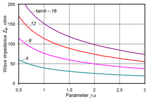
Figure 4 Wave impedance Z0 versus parameter γa for different values of angle Φ.

Equating the right hand sides of (33) and (35) leads to the dispersion equation (26), which confirms the equivalence of both expressions for the wave impedance. Figure 4 illustrates the dependence of the wave impedance on the dimensionless parameter γα calculated for the free helix for different values of Φ. It is seen that Z0 increases with the increase in Φ. It is obvious that in the presence of a solid cylindrical screen electrode the equivalent capacitance will increase and the equivalent inductance will decrease, producing a corresponding decrease in the wave impedance. This effect depends strongly on the value of γα, increasing with decreasing γα, i.e. with decreasing frequency, which in turn leads to a flattening the dependence of Z0 on frequency.

Calculation of the power flow by differentiation

In practice, when SWS has two or more cross-sectional areas, the calculation of the power flow is the most difficult part of the analysis. The same calculation is required for evaluation of the interaction impedance K1 and the coupling coefficient Kc,18 both values being used in the TWT theory for evaluation of the electron beam interaction with a slow wave. Being dimensionless, Kc is more convenient for practical application. In the case of a cylindrical beam tunnel with radius a filled by an electron beam18

K c = ω ε 0 π a 2 2 β 0 P A 2 [ I 0 2 ( γ 0 a) I 1 2 ( γ 0 a)] MathType@MTEF@5@5@+= feaagKart1ev2aaatCvAUfeBSjuyZL2yd9gzLbvyNv2CaerbuLwBLn hiov2DGi1BTfMBaeXatLxBI9gBaerbd9wDYLwzYbItLDharqqtubsr 4rNCHbGeaGqiVu0Je9sqqrpepC0xbbL8F4rqqrFfpeea0xe9Lq=Jc9 vqaqpepm0xbba9pwe9Q8fs0=yqaqpepae9pg0FirpepeKkFr0xfr=x fr=xb9adbaqaaeGaciGaaiaabeqaamaabaabaaGcbaqcLbsacaWGlb qcfa4aaSbaaKqaGeaajugWaiaadogaaSqabaqcLbsacqGH9aqpjuaG daWcaaGcbaqcLbsacqaHjpWDcqaH1oqzjuaGdaWgaaqcbasaaKqzad GaaGimaaWcbeaajugibiabec8aWjaadggajuaGdaahaaWcbeqcbasa aKqzadGaaGOmaaaaaOqaaKqzGeGaaGOmaiabek7aILqbaoaaBaaaje aibaqcLbmacaaIWaaaleqaaKqzGeGaamiuaaaacaWGbbqcfa4aaWba aSqabKqaGeaajugWaiaaikdaaaqcLbsacaGGBbGaamysaKqbaoaaDa aajeaibaqcLbmacaaIWaaajeaibaqcLbmacaaIYaaaaKqzGeGaaiik aiabeo7aNLqbaoaaBaaajeaibaqcLbmacaaIWaaaleqaaKqzGeGaam yyaiaacMcacqGHsislcaWGjbqcfa4aa0baaKqaGeaajugWaiaaigda aKqaGeaajugWaiaaikdaaaqcLbsacaGGOaGaeq4SdCwcfa4aaSbaaK qaGeaajugWaiaaicdaaSqabaqcLbsacaWGHbGaaiykaiaac2faaaa@723C@ , (36)

Where the power flow P is calculated by integrating the Pointing flux across the cross-section of the SWS, while the phase constant β0 and transverse constant γ0 are defined in the absence of the electron beam. It follows from (36) that

P= ω ε 0 π a 2 A 2 2 β 0 I 0 2 ( γ 0 a) I 1 2 ( γ 0 a) K c MathType@MTEF@5@5@+= feaagKart1ev2aaatCvAUfeBSjuyZL2yd9gzLbvyNv2CaerbuLwBLn hiov2DGi1BTfMBaeXatLxBI9gBaerbd9wDYLwzYbItLDharqqtubsr 4rNCHbGeaGqiVu0Je9sqqrpepC0xbbL8F4rqqrFfpeea0xe9Lq=Jc9 vqaqpepm0xbba9pwe9Q8fs0=yqaqpepae9pg0FirpepeKkFr0xfr=x fr=xb9adbaqaaeGaciGaaiaabeqaamaabaabaaGcbaqcLbsacaWGqb Gaeyypa0tcfa4aaSaaaOqaaKqzGeGaeqyYdCNaeqyTduwcfa4aaSba aKqaGeaajugWaiaaicdaaSqabaqcLbsacqaHapaCcaWGHbqcfa4aaW baaSqabKqaGeaajugWaiaaikdaaaqcLbsacaWGbbqcfa4aaWbaaSqa bKqaGeaajugWaiaaikdaaaaakeaajugibiaaikdacqaHYoGyjuaGda WgaaqcbasaaKqzadGaaGimaaWcbeaaaaqcfa4aaSaaaOqaaKqzGeGa amysaKqbaoaaDaaajeaibaqcLbmacaaIWaaajeaibaqcLbmacaaIYa aaaKqzGeGaaiikaiabeo7aNLqbaoaaBaaajeaibaqcLbmacaaIWaaa leqaaKqzGeGaamyyaiaacMcacqGHsislcaWGjbqcfa4aa0baaKqaGe aajugWaiaaigdaaKqaGeaajugWaiaaikdaaaqcLbsacaGGOaGaeq4S dCwcfa4aaSbaaKqaGeaajugWaiaaicdaaSqabaqcLbsacaWGHbGaai ykaaGcbaqcLbsacaWGlbqcfa4aaSbaaKqaGeaajugWaiaadogaaSqa baaaaaaa@712E@ , (37)

That at known already Kc makes it possible calculating P. There are relatively simple methods for calculating Kc by differentiation the dispersion equation in the presence of the electron beam:18,20

K c = γ 0 2 β 0 2 ( | dT dγ | γ 0 1) 1 MathType@MTEF@5@5@+= feaagKart1ev2aaatCvAUfeBSjuyZL2yd9gzLbvyNv2CaerbuLwBLn hiov2DGi1BTfMBaeXatLxBI9gBaerbd9wDYLwzYbItLDharqqtubsr 4rNCHbGeaGqiVu0Je9sqqrpepC0xbbL8F4rqqrFfpeea0xe9Lq=Jc9 vqaqpepm0xbba9pwe9Q8fs0=yqaqpepae9pg0FirpepeKkFr0xfr=x fr=xb9adbaqaaeGaciGaaiaabeqaamaabaabaaGcbaqcLbsacaWGlb qcfa4aaSbaaKqaGeaajugWaiaadogaaSqabaqcLbsacqGH9aqpjuaG daWcaaGcbaqcLbsacqaHZoWzjuaGdaqhaaqcbasaaKqzadGaaGimaa qcbasaaKqzadGaaGOmaaaaaOqaaKqzGeGaeqOSdi2cdaqhaaqcbasa aKqzadGaaGimaaqcbasaaKqzadGaaGOmaaaaaaqcLbsacaGGOaqcfa 4aaqWaaOqaaKqbaoaalaaakeaajugibiaadsgacaWGubaakeaajugi biaadsgacqaHZoWzaaaakiaawEa7caGLiWoajuaGdaWgaaWcbaqcLb sacqaHZoWzjuaGdaWgaaqccasaaKqzadGaaGimaaadbeaaaSqabaqc LbsacqGHsislcaaIXaGaaiykaKqbaoaaCaaaleqajeaibaqcLbmacq GHsislcaaIXaaaaaaa@61AE@ . (38)

Here T is the transverse constant in the electron beam and γ is the "disturbed" by the beam transverse constant in free from the electrons areas. This gives for the free helix interacting with the electron beam with radius α:

K c = τ 0 2 β 0 2 I 0 2 ( γ 0 a) I 1 2 ( γ 0 a) I 0 ( γ 0 a) K 0 ( γ 0 a) F( γ 0 a) γ 0 a ] MathType@MTEF@5@5@+= feaagKart1ev2aaatCvAUfeBSjuyZL2yd9gzLbvyNv2CaerbuLwBLn hiov2DGi1BTfMBaeXatLxBI9gBaerbd9wDYLwzYbItLDharqqtubsr 4rNCHbGeaGqiVu0Je9sqqrpepC0xbbL8F4rqqrFfpeea0xe9Lq=Jc9 vqaqpepm0xbba9pwe9Q8fs0=yqaqpepae9pg0FirpepeKkFr0xfr=x fr=xb9adbaqaaeGaciGaaiaabeqaamaabaabaaGcbaqcLbsacaWGlb qcfa4aaSbaaKqaGeaajugWaiaadogaaSqabaqcLbsacqGH9aqpjuaG daWcaaGcbaqcLbsacqaHepaDlmaaDaaajeaibaqcLbmacaaIWaaaje aibaqcLbmacaaIYaaaaaGcbaqcLbsacqaHYoGylmaaDaaajeaibaqc LbmacaaIWaaajeaibaqcLbmacaaIYaaaaaaajuaGdaWcaaGcbaqcLb sacaWGjbWcdaqhaaqcbasaaKqzadGaaGimaaqcbasaaKqzadGaaGOm aaaajugibiaacIcacqaHZoWzjuaGdaWgaaqcbasaaKqzadGaaGimaa WcbeaajugibiaadggacaGGPaGaeyOeI0IaamysaSWaa0baaKqaGeaa jugWaiaaigdaaKqaGeaajugWaiaaikdaaaqcLbsacaGGOaGaeq4SdC wcfa4aaSbaaKqaGeaajugWaiaaicdaaSqabaqcLbsacaWGHbGaaiyk aaGcbaqcfa4aaSaaaOqaaKqzGeGaamysaKqbaoaaBaaajeaibaqcLb macaaIWaaaleqaaKqzGeGaaiikaiabeo7aNLqbaoaaBaaajeaibaqc LbmacaaIWaaaleqaaKqzGeGaamyyaiaacMcaaOqaaKqzGeGaam4saK qbaoaaBaaajeaibaqcLbmacaaIWaaaleqaaKqzGeGaaiikaiabeo7a NLqbaoaaBaaajeaibaqcLbmacaaIWaaaleqaaKqzGeGaamyyaiaacM caaaqcfa4aaSaaaOqaaKqzGeGaamOraiaacIcacqaHZoWzjuaGdaWg aaqcbasaaKqzadGaaGimaaWcbeaajugibiaadggacaGGPaaakeaaju gibiabeo7aNLqbaoaaBaaajeaibaqcLbmacaaIWaaaleqaaKqzGeGa amyyaaaaaaGaaiyxaaaa@8F1C@ . (39)

For the free helix, the coupling coefficient was defined with the help of formula (36) in the monograph.18 The substitution (39) in (37) gives an expression for P identical to that obtained in1 and18 by integration the power flow density.

Discussion

A method of replacing the slow-wave structure by an equivalent transmission line with parameters providing unambiguous determination of the wave impedance was found and described. The method is based on the introduction of an equivalent voltage that yields the correct value of power flowing for the real value of the conduction current. It is shown that the decrease in the equivalent inductance and simultaneous increase in the equivalent capacitance, proportional to the decrease in the equivalent voltage, provides an unambiguous definition of the wave impedance. The decrease in the equivalent voltage is defined by the decrease in the real power flow, caused by the longitudinal capacitive currents.

It is demonstrated also that the unambiguous determination of the wave impedance of slow-wave structures can be simplified by differentiation of the dispersion equation in the presence of a homogeneous electron beam.

Acknowledgements

The author wishes to thank Dr. David Chernin of Leidos for editorial and English grammar assistance.

Conflict of interest

The author declares no conflict of interest.

References

  1. JR Pierce. Traveling Wave Tubes Prinston. Van Nostrand, NJ, USA; 1950.
  2. Lebedev IV. Microwave Technology and Devices. Vysshaya Shkola, Moscow, Russia; 1970.
  3. Collin RE. Foundations for Microwave Engineering. USA: McGraw–Hill Book Company; 1992.
  4. Neiman MS. Generalizing the circuit theory on the waveguides. Gosenergoizdat, Moscow, Russia; 1955.
  5. Brown RG, Sharpe RA, Hughes WL, et al. Lines, Waves, and Antennas. The Transmission of Electric Energy. 2nd ed. USA: John Wiley & Sons; 1973.
  6. Silin RA, Sazonov VP. Slow–Wave Structures. Sovradio, Moscow, Russia; 1966.
  7. Pike SF. Design formulas for helix dispersion shaping. IEEE Transactions on ED. 1969;16(12):1010–1014.
  8. Yu N Pchelnikov. Relationship between the wave impedance and the coupling resistance of slow–wave structures. Radiotekhnika i Electronika. 1983;28(10):1981–1985.
  9. Gilmour S. Principles of raveling Wave Tubes Boston London: Artech House, London, UK; 1994.
  10. Carter RG, Wang P. An equivalent circuit model for helix slow–wave structures. Proc Conf Microwaves. 1994:94.
  11. Watkins DA. Topics in Electromagnetic Theory. USA: John Willy & Sons Inc; 1958.
  12. Yu N Pchelnikov. Features of slow–waves and potentials for their nontraditional application. Journal of Communication Technology and Electronics. 2003;48(4):450–462.
  13. Pchelnikov Yu N, Kholodnyi VA. Medical Application of Surface Electromagnetic Waves. Bioelectrochemistry and Bioelectronics. 1988;47(2):283–290.
  14. Yu N Pchelnikov, Nyce DS. Slow–wave structures based method of measurements. IEEE Trans on Instrum Measur. 2002;51(5):891–896.
  15. Yu N Pchelnikov. Sensitive element on cross–wound helices. IEEE Sensors Journal. 2017;17(9):1–7.
  16. Yuriy N Pchelnikov. Determination of equivalent parameters of waveguides with circular and rectangular cross sections. Journal of Communication Technology and Electronics. 2010;55(1):106–111.
  17. Yu N Pchelnikov, Ye V Zykova, N Ye Ivanova. On a procedure for determining the parameters of equivalent circuits. Radiotekhnika i Electronikas. 1980;25(6):1231–1237.
  18. Loshakov LN, Yu N Pchelnikov. Theory and Gain Calculation of Traveling Wave Tube. Sovradio, Moscow; 1964.
  19. Yu N Pchelnikov. On the replacement of slow–wave systems by a three–conductor equivalent line. Journal of Communication Technology and Electronics. 1994;39(9):68–74.
  20. Yu N Pchelnikov. Calculation of the coupling coefficient of electron beam in TWTs using parameters of equivalent line. Journal of Communication Technology and Electronics. 2010;55(2):215–220.
Creative Commons Attribution License

©2017 Pchelnikov. This is an open access article distributed under the terms of the, which permits unrestricted use, distribution, and build upon your work non-commercially.