Derivation of energy spectrum in presence of an external electric field
For an external electric field (f) applied along the x-axis, the perturbed Hamiltonian (H'), can be forwarded as
(1)
Where,
and e is the electron charge. The second order energy Eigen-value,
under perturbation condition, Eqn (1) is given as6
(2)
where,
(3)
(4)
(5)
H is the total Hamiltonian,
is the wave function with
as the periodic function of it.
, n, ,
E and
are the un-perturbed Hamiltonian, the band index, the position vector of electron, the wave vector of the electron, the total energy of the electron and the energy of an electron in the periodic lattice, respectively. For a semiconductor having parabolic energy band, we get from Eqns (1) and (2)
……….. (6)
= …………. (7)
………….. (8)
Where
is the x-component of
and the integration in Eqn (8) extends over the unit cell. From Eqns (6)-(8), with n-corresponding to conduction band
and m, corresponding to valence band
Eqns 6 can be reproduced as
……….. (9)
where,
……(10)
is the un-perturbed parabolic conduction band with is the effective electron mass at the band-edge of the CB.
is the reduced Planck’s constant, given by
.
and Xcv are the intra and interband transition matrix elements, respectively. For the evaluation of
and
, we use
.
Perturbation technique7 for the isotropic two-band model. The two-bands are separated by the energy gap, Eg at
accordingly, we find
……….. (11)
………. (12)
and mr is the reduced electron effective mass, given by
………….(13)
Combining the appropriate equations, the electron energy-spectrum in the presence of an external electric field, can be put forward, as.3
……… (14a)
where,
………… (14b)
Equations (14a) and (14b) show that in the presence of an external electric field, the isotropic parabolic un-perturbed energy-spectrum, (Eqn 10), exhibits an anisotropic dispersion relation, with energy dependent mass anisotropy in the presence of an external electric field. This anisotropic dispersion relation transform to an isotropic one under the approximation:
.……. (15)
Under this, Eqn (14a) turns out to the isotropic dispersion relation:
……. (16)
Further, in the limiting case, when
i.e; at the band-edge, Eqn(16) provides the results:
……… (17)
From Eqn.17, it is clear that in the presence of an electric field, F, the conduction band-edge moves vertically up-word by an amount, ΔE. As a result, the band-gap of semiconductor is apparently increased by ΔE, when an external electric field is applied. This observation is opposite to the Franz8 and Keldysh9 effects, a phenomena where the band-gap decreases by means of an applied electric field. In support of our theoretical findings, the experimental observation of the band-gap enhancement with the electric field can be found in.10–12
Derivation of energy-spectrum in presence of an electric and parallel magnetic fields
In the presence of a parallel magnetic field, B, applied along the direction of the electric field, the transverse component of electron energy,
is quantized by Landau quantization5 as
…..(18)
Where,
is the transverse or normal component of wave vector, J is the Landau quantum number;
is cyclotron energy, given by
………(19)
and g is the difference in spin g-factors of conduction and valence band
and
is the Bohr’s magnetron.
………. (20)
Generally, the magnitude of the transverse component of electron energy, E is given as
. Under this condition, we can approximate
in Eqn(11). Therefore, combining Equation (9)-(12), we can approximately write Eqn (16).
+ ……(21)
For
we find from Eqns (16) - (18)
……….. (22)
Combining Eqns (16), (18)-(21), we get
……(23)
.……..(24)
Equations (23) and (24) represent the E- kx dispersion relation of conduction electron in presence of electric and parallel magnetic fields. From Eqns (23) and (24), we find that the parabolic energy-band no more remains to the parabolic shape but is quantized by means of electric as well as parallel magnetic fields. Under the limiting conditions,
we find from Eqn 21 the new increased band gaps
of semiconductor in presence of electric and parallel magnetic fields.
……..(25)
Under the case, when
and
We find from Eqns (23)-(25), the increased band-gap
in presence of electric field only same as Eqn (17). Combining Eqns (17) and (25), we find that the increased band-gap value of semiconductor in the presence of electric field and a parallel magnetic field of greater that the value, when only electric field is present, i.e.,
Derivation of the density –of-states (DOS) functions in presence of electric as well as with the presence of electric and parallel magnetic fields
The density-of-states, N (E, F), in presence of electric field (F) can be written from Eqns. (14a) and (14b) as3
.………. (26)
Where
……………. (27)
In the absence of electric field, N (E, 0) assumes the well-known form,13 from Eqns. (26) and (27), as
……. (28)
Now, from Eqns (24) and (25), the density-of-states, N (E, F, B) in the presence of electric and parallel magnetic fields, is given as (for conduction band, CB)
……..(29)
Where,
…. (30)
i.e. cyclotron of an energy spectrum an electron in the conduction band,
=Maximum value of Landau quantum number,
Integer value of
In the limiting case, when
Eqns (29 and 30) will lead to the well-known form for (CB) as13
…… (31)
Using the appropriate equations and taking n-GaAs as an example, together with the parameters,13
and
we have plotted the energy-spectrum versus electron wave-vector
shown in Figure 1, in the presence of electric field (f). This Figure 1 is plotted following Eqn. (16). The curve passes through origin, i.e., E=0 and
This is the case of un-perturbed band. The amount of shift of the band-edge at
with electric field,
is given by Eqn. (17). Therefore, it is clear that the parabolic nature of the original band is modified to a large extent due to the electric field. It further appears that as the electric field is increased, the edge of the conduction band (CB) moves vertically in the positive energy direction. Consequently, the band-gap is increased with the electric field.
Franz8 and Keldysh9 effects, conventionally implies that the band-gap of a semiconductor decreases with the application of an electric field. Incidentally, in accordance with our calculations, Eqns (14a)-(17) and Figure 1, we observe that the Franz-Keldysh effects are directly the opposite one. The physical explanation in support of the above observation can be given, based on our works on optical absorption in the presence of an external electric field.12

Figure 1 Plots of Energy-Spectrum, E (in eV) against
(wave vector in atomic unit, 108 cm-1) for n-GaAs at 300K for f=0.0 V cm-1 (dotted curve),
and
(solid line).
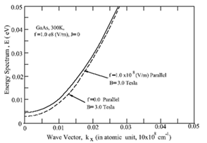
In Figure 2, we have plotted the electron energy- spectrum against wave-vector
(in atomic unit) for the electric field,
and B=3.0 Tesla (dotted line); and
Tesla (Solid line); under extreme quantum limit, i.e., J=0. Figure 2 is plotted following Eqns (24) and (25). It is clear from Figure 2 that the dotted curve does not pass through origin; but shifting from it by an amount equal to (1/2)
This shows that the band-gap increase with magnetic field, which is the well-known result. However, for the solid curve, the value of the electron energy (E) further increases with the electric field as well as magnetic fields. As we move deep into the band. For
(a.u) the curves merged to each other. From Figure 2, we may conclude that in the presence of magnetic field, the Landau sub-bands are formed and at
the band-edge of semiconductor moves vertical upward, indicating the increase of band-gap value with the magnetic field. The increase of band-gap value is further enhanced by the electric field, when both electric and parallel magnetic fields are simultaneously present.

Figure 2 Plots of Energy-Spectrum, E (in eV) against
(x-component of wave vector in atomic unit,
1) for n-GaAs at 300K for B=3.0 Tesla (dotted curve),
and B= 3.0Tesla (solid line).
Figure 3 has been plotted for the density-of-states (DOS), N (E, F), (normalized by
against electron energy E (in eV) under various values of electric field,
We may infer from this that, for
the curve (solid line) passes through the origin. For finite values of the electric energy (E) axis; besides the curves of (N (E, F) are flattened with respect to f=0.0 Vcm-1 case. It is to be noticed that, we cannot apply the electric field F (= e.f) to an arbitrary values, the maximum possible value of
must be limited by:
where
is the band-gap of semiconductor (in eV), “e” is the electron charge and “d” is the lattice constant of semiconductor. This is because for the electric field
there is a possibility of lattice break-down to happen. So, we must limit the value of electric field strength
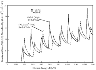
Referring to Figure 4 plots are made for n-GaAs at 300K for the following cases:
- N (E, F, B) (DOS, normalized by 1.6 ×1018 cm-3/eV) vs electron energy, E (eV), in presence of f=0.0 (V cm-1) and a parallel magnetic field, B=3.0 Tesla.
- For N (E, F, B) vs electron energy, E (eV), in presence of f=1.6×106cm-3/eV and a parallel magnetic field, B=3.0 esla.
- From Figure 4, following remarks might be noticed: (a) in both the graphs (1) and (2), the natures of variations of DOS functions with the electron energy (E) are similar with showings singularities. (b) the positions of the singularity points, (Dotted curves, for the case to when F B are present) are shifted to a higher electron energy E(eV) than case when only magnetic field ‘B’ is present marked by solid lines. Since, we conclude from these graphs that in the study of magneto-resistance, the phase value with F B are higher than the case when only magnetic field (B) is present.

Figure 3 Plots for density-of-state function, N (E, F) (normalized by a factor
against electron energy, E (in eV) for n-GaAs under various electric fields, f.

Figure 4 Plots of density-of-states function, N (E, F, B) against electron energy, E (in eV) for n-GaAs at 300K for
) and B=3.0 Tesla (solid curves) and
and B=3.0 Tesla (dotted curves).
Referring to Figure 5, it appears that DOS function, N(E,F) varies with more or less constant values against electric field (up to a certain value), for different values of Electron energy, E. Thereafter, the rates of fall of N (E, F) value (in magnitude) increases with electron energy (E). Finally, the value of N (E, F) approaches to zero, implying thereby that the carriers disappear near the conduction band (CB) edge, as the applied electric field increase.3 Similar types of vanishing of the carriers have been observed in (CB) experimentally by Miyazawa and Ikoma.14 In Figure 6, we have plotted DOS function, N (E, F, B) [normalized by a factor of 1.6×10¹⁸(cm3/eV), against electric field, f(Vcm-1), for electron energy, E=30meV and a parallel magnetic field, B=3.0 Tesla for n-GaAs at 300K. It is shown in Figure 6, that the DOS function is almost a constant value over a certain values of the variation of the electric field. Therefore, as the electric field f is further increased the values of DOS decreases with oscillations and finally approaches to zero value. This implies that in the presence of an electric field and parallel magnetic fields, the availability of the carriers disappear from the CB edge with oscillations due to magnetic field. This phenomenon is unlikely to the cases; only when electric field is present and absence of magnetic fields (Figure 5).

Figure 5 Plots of density-of-State function, N (E, F) (normalized by a factor,
) for n-GaAs against electric field f (in Vcm-1) for E=1.0(meV), 10.0 meV) and 50(meV).
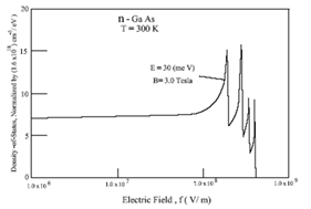
Figure 6 Plots of density-of-State function, N (E, F, B) (normalized by a factor,
) for n-GaAs against electric field f (in vcm-1) for E=30(meV), B=3.0 Tesla.


