eISSN: 2574-9927


Research Article Volume 4 Issue 5
1Department of Civil and Environmental Engineering, New Jersey Institute of Technology, USA
2Interdisciplinary Program in Materials Science & Engineering, New Jersey Institute of Technology, USA
Correspondence: Ravindra NM, Department of Civil and Environmental Engineering, New Jersey Institute of Technology, Newark, New Jersey 07102, USA
Received: October 07, 2020 | Published: October 21, 2020
Citation: Leqi L, Ravindra NM. Simulation of optical properties of semiconductor multilayers from extreme ultraviolet to far infrared. Material Sci & Eng. 2020;4(5):131-137. DOI: 10.15406/mseij.2020.04.00139
Optical properties of semiconductors play a critical role in various applications including the design and manufacture of optical components, devices & sources, energy conversion and process monitoring & control. While the fundamental understanding of the optical properties of semiconductors has grown over the years, reliable data of the optical constants of semiconductors, particularly in the infrared range of wavelengths, is severely lacking in the literature. In this overview, detailed case studies of the optical properties of Silicon on Insulator (SOI) and Ge photodetectors, based on Forouhi-Bloomer dispersion equation, as function of photon energy (or wavelength) and thickness are presented. The obtained simulation results, based on this relation, are in good accord with the literature values and are consistent with some well-accepted studies. Furthermore, the results reported in this analysis are helpful for the determination and realization of the optical response of materials under conditions of varying photon energy and thickness.
Optical properties of semiconductors play a critical role in various applications including the design and manufacture of optical components & devices such as detectors, filters, imagers, lenses, optical coatings, photonic crystals, sensors and waveguides, sources such as lasers & light emitting diodes, energy conversion, process monitoring & control using in situ, non-contact techniques such as radiation pyrometry, spectroscopic ellipsometry and time resolved reflectivity. While the fundamental understanding of the optical properties of semiconductors has grown over the years, reliable data of the optical constants of semiconductors, particularly in the infrared range of wavelengths, is severely lacking in the literature. In order to meet the unprecedented demands for advanced high-speed semiconductor devices, silicon-based materials such as silicon-on-insulator (SOI) and silicon on sapphire (SOS) substrates have attracted considerable interest due to significant transformation of their optical and electrical properties caused by quantum-confinement effects. Silicon is an excellent material system for optical confinement and wave transmission in the near infrared range1 and SiO2 has good compatibility with the existing CMOS technology for microelectronics and photonics.2 High quality Ge crystals have been used for highly sensitive near-infrared (NIR) photodetectors in the radiation wavelength of 1300-1600 nm,3 and exhibit significant absorption in the telecommunication wavelengths range.4 Ge photodetectors are the first active optoelectronic devices monolithically integrated on Si5 and have revolutionized optical communications. Their performance is comparable to III-V semiconductor detectors (e.g., InGaAs) due to their shorter absorption lengths, higher electron mobilities, faster response times and lower power dissipation.3
Modeling the radiative properties of semiconductor multilayers such as SOI structures and Ge photodetectors is important in several areas of optoelectronics in the desired near-infrared (NIR) range of wavelengths. These material structures are used in light detectors, waveguides and other optical applications. Optical dispersion depends on the incident photon energy (E) or wavelength of light (λ), as well as on the material properties and the device fabrication conditions. Optical properties can be expressed as the real and imaginary parts of the complex index of refraction relation as N = n - ik, where n is the refractive index and k is the extinction coefficient. Optical functions, n and k, are intrinsic material properties and may be thought of as the fingerprint of a material, and cannot be measured directly.6 They are determined from extrinsic measurements that depend on their surface morphology, dopant type and dopant concentration /resistivity etc. (e.g., reflectance and transmittance, or ellipsometric parameters). In this study, an investigation of the optical properties of semiconductors, based on the Forouhi–Bloomer dispersion equations for n and k, is presented by utilizing the experimental fitting parameters in the literature, for material component layers in SOI and Ge photodetector structures. Furthermore, the transmittance, reflectance, absorbance and emissivity are calculated based on the obtained n and k. By understanding the optical and electrical properties, their behavior, as function of thickness and photon energy (or wavelength) for these multilayers, is predicted. The results of these simulations can be used to engineer these multilayers for various applications in optoelectronics.
Forouhi-Bloomer dispersion equation for k(E) and n(E)
Spectroscopic ellipsometry (SE) is a well-established optical technique that is utilized to characterize the optical functions and other related properties by performing the measurement of the relative phase change of reflected and polarized light.7 Refractive index (n) describes the behavior of light propagating through the medium, which is normally defined as n = [c/v], where c is the speed of light in vacuum and v is the phase velocity of light in the medium. Extinction coefficient, k, characterizes the ability of the light beam to penetrate into the material. The Forouhi-Bloomer dispersion equation,6 applicable to the entire wavelength from radio-wave to EUV spectral range, is proposed as in Eq. (I) and Eq. (II) for k(E) and n(E), respectively.8,9 This dispersion model is consistent with the Kramers–Kronig analysis.
Eq. (I)
Eq. (II)
where ;
;
;
.
The fitting parameter, Ai, in Eq. (I) is a dimensionless contant, which represents the amplitude of transition based on the transition probability. The quantity, Bi, is the energy difference between the initial and final states involved in the electron transition. The quantity Cj = [(B2/4) + (ħ2/2τj )], where τj represents the lifetime of the j th excited electron state. The number of terms p and q are taken as the quantity of peaks in k(E).
Emissivity and absorption coefficient
After obtaining the extinction coefficient and refractive index from the experimental measurements of transmittance [T(λ)] and reflectance [R(λ)], they can be calculated exactly, irrespective of the number of layers or differences between the angles of incidence. These quantities are wavelength dependent. The expression for the absorption coefficient (α) of the multilayers is given by Eq. (III).
Eq. (III)
where, k is the extinction coefficient.
The optical transmittance, which is an effective and accurate pathway to obtain the optical constants below the absorption edge, can be measured or calculated by Eq. (IV),
Eq. (IV)
where, t is the thickness of the material. The reflectance can be obtained from Eq. (V) and Eq. (VI),
Eq. (V)
and
Eq. (VI)
where, n is the refractive index of the first layer, s is the refractive index of the second layer and k is the extinction coefficient. Emissivity (ε) is a parameter that identifies the radiative properties of materials under conditions of thermal (temperature) equilibrium with the ambient.10 It can be obtained from reflectance (R) and transmittance (T) of a layer as in Eq. (VII). From this, the absorptance, and hence the emissivity, is determined using A = 1 – [T + R].
Eq. (VII)
Silicon on Insulator (SOI)
In this study, the radiative properties of SOI structures, based on the earlier studies of Ravindra et al11 on SIMOX (Separation by IMplanted Oxygen) structures, with 200-nm Si/400-nm SiO2/ Si-substrate, as the control group, are considered to demonstrate the validity of the proposed simulation model. In Figure 1a, a case study, based on Li et al12 considering the thickness of Si as 1000 nm on top of a 2000 nm thick SiO2, is presented. Another case study is based on Badri et al13 with the thickness of SiO2 as 2000 nm with the top layer of Si varying in thickness from 75 to 325nm. The investigation of the detailed optical properties of SOI structures, based on these two case studies, are presented as a function of thickness and photon energy (or wavelength). The simulations are implemented in MATLAB using the fitting parameters based on Forouhi-Bloomer dispersion model for the refractive index and extinction coefficient of Si and SiO2 and are summarized in Table 1.
|
Experimental data |
Number of terms for the calculations |
Ai (eV) |
Bi (eV) |
Ci (eV2) |
n (¥) |
Eg (eV) |
|
Si (1.5-6eV)9 |
q=4 |
0.00405 |
6.885 |
11.864 |
1.95 |
1.06 |
|
|
|
0.01427 |
7.401 |
13.754 |
|
|
|
|
|
0.0683 |
8.634 |
18.812 |
|
|
|
|
|
0.17488 |
10.652 |
29.841 |
|
|
|
SiO2(0.031-25eV) 6 |
p=5 |
5.1915E-04 |
1.1489E-01 |
3.3119E-03 |
1.05 |
|
|
|
|
1.59E-04 |
1.95E-01 |
9.53E-03 |
|
|
|
|
|
6.4532E-04 |
2.699E-01 |
1.8245E-02 |
|
|
|
|
|
5.7594E-05 |
2.9619E-01 |
2.1951E-02 |
|
|
|
|
|
2.5000E-01 |
0 |
3.8183 |
|
|
|
|
q=4 |
5.7165E-02 |
2.0661E+01 |
1.068E+02 |
|
9.0 |
|
|
|
1.4334E-01 |
2.3394E+01 |
1.3749E+02 |
|
|
|
|
|
4.3659E-02 |
2.7231E+01 |
1.8623E+02 |
|
|
|
|
|
2.1804 |
3.0863E+01 |
2.6368E+02 |
|
|
|
|
|
0.05366 |
21.940 |
125.443 |
|
|
|
Ge (0.5-7eV) 9 |
q=4 |
0.00103 |
4.313 |
4.654 |
2.161 |
0.6 |
|
|
|
0.11637 |
4.677 |
5.639 |
|
|
|
|
|
0.10968 |
6.728 |
11.858 |
|
|
|
|
|
0.03479 |
8.704 |
19.119 |
|
|
|
Si0.95Ge0.0514 |
P=1 |
0.0022 |
6.8 |
11.7 |
1.79 |
|
|
|
q=3 |
0.083 |
7.3 |
14.1 |
|
1.08 |
|
|
|
0.012 |
8.6 |
18.7 |
|
|
|
|
|
0.061 |
10.7 |
30.2 |
|
|
|
Si0.9Ge0.114 |
P=1 |
0.0061 |
6.7 |
11.4 |
1.05 |
|
|
|
q=3 |
0.37 |
6.4 |
15.8 |
|
1.05 |
|
|
|
0.012 |
8.4 |
18.1 |
|
|
|
|
|
0.13 |
10.5 |
38.4 |
|
|
|
Si0.85Ge0.1514 |
P=1 |
0.014 |
6.6 |
11.2 |
1.11 |
|
|
|
q=3 |
0.7 |
5.3 |
15.1 |
|
1.01 |
|
|
|
0.02 |
8.5 |
18.2 |
|
|
|
|
|
0.079 |
8.8 |
23.02 |
|
|
Table 1 Fitting parameters of F-B dispersion model
Ge-on-Si photodetectors
Here, we investigate the optical properties of several Ge based photodetectors, Si/Ge/Si and Si/Ge/SOI, as shown in Figure 1b & 1c, as a function of thickness and photon energy (or wavelength). The thickness of Ge layer is varied from 400 to1200 nm in steps of 200nm (i.e., 400, 600, 800, 1000, 1200 nm) and the thickness of bulk Si or SOI substrates consisting of thin SiO2 and silicon layer (150nm Si on 400nm SiO2 decreasing to 60nm Si on 150nm SiO2)14 are considered. Besides, another interesting case study, based on Chong et al12 on coupled waveguides of Ge-on-SOI (Si/Ge/Si/Si/SiO2/Si), as shown in Figure 1d, with the thickness of Si (100nm), Ge (1000nm), Si(600 nm), Si(220nm) and SiO2 (2000nm), respectively, is investigated. Besides the Ge photodetector, we also report the optical properties of GexSi1-x (x = 0.05, 0.1 and 0.15) alloys on Si by varying the thickness of GexSi1-x from 100-1000 nm based on the case study of Kadri et al15 The simulations are implemented in MATLAB using fitting parameters based on Forouhi-Bloomer dispersion model for the n and k of Si, Ge, SiGe and SiO2, as shown in Table 1.
Silicon on insulator
The refractive index (n) and extinction coefficient (k), and their wavelength dependence, are the required fundamental properties for optical design of a variety of structures for applications in energy, optics and optoelectronics. These properties, as function of photon energy (or wavelength), for Si and SiO2, obtained from the Forouhi–Bloomer dispersion equation, are considered in these simulations. By inspecting the n and k spectra of each material, the entire dispersion pattern can be categorized into three distinct regions – near IR (NIR) energies (10-2 to 1.0eV), NIR to UV energies (1.0eV to 7eV) and UV to EUV (Extreme UV) energies (>7eV). In Figure 2a, it is observed that n of Si increases when the photon energy is >1eV, attaining a peak value of 6.7 at 3.5eV; then, it decreases subsequently. k of Si shows a similar dependence on photon energy as n; k increases when the energy is > 3.2eV, reaching the peak value of 5.3 at 4.3eV, then decreases to almost 0. Both n and k of Si are consistent with the results of Forouhi et al.9 In Figure 2b, n of SiO2 glass exhibits two peak values – one peak in the energy range of 0.06-0.16eV and another peak value of 2.45 at 10eV, which may be due to the inter-band absorption.6 k of SiO2 has almost a similar pattern as n; the behavior of both k and n, with photon energy, are consistent with those of Forouhi et al.6
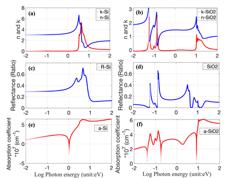
Figure 2 Simulation of n and k for (A) Si and (B) SiO2; optical reflectance of (C) Si and (D) SiO2; absorption coefficient of (E) Si and (F) SiO2 as function of energy.
In Figure 2c, the reflectance of Si has a high value of >60% in the energy range of 3.2-5.6eV (~ 220-400nm (UVA to UVC)). In Figure 2d, the reflectance of SiO2 exhibits several peaks with values >20% from 0.06-5eV. It can be concluded that the reflectance of SiO2 is highly related to the varying n, and the reflectance of Si is related to both n and k. Several studies in the literature have confirmed the correlation of reflectance of materials with their surface roughness, measured using Atomic Force Microscopy;14 for example, Xie et al16 showed that the reflectance is strongly related to the surface morphology of three-dimensional germanium islands on Si(100) substrates. The dependence of the absorption coefficient of Si and SiO2, as function of energy, are shown in Figures 2e & 2f respectively. Both of them have high values > 6x107 cm-1 for E>4eV. In order to establish the validity of the simulations, in Figures 3a-3d, a case study of SIMOX, based on Ravindra et all11 has been considered (200-nm Si/ 400-nm SiO2/ 700-µm p-Si). In this Figure 3, the experimentally measured reflectance (Figure 3a), transmittance (Figure 3d), and emittance spectra (Figure 3B), of SIMOX are compared with the results from our modeling and simulations (Figure 3c). A case study, based on Li et al12 with the thickness of top Si layer varying from 75-1000 nm on 2000 nm SiO2 and Si as the substrate is simulated and presented in Figure 4. The results show that the SOI structures exhibit similar patterns with slight change in emissivity from 20% to 40% with the thickness of Si varied from 75nm-1000 nm. On the other hand, in Figure 5, SOI structures exhibit significant changes in emissivity, transmittance and reflectance in the wavelength range of 7–22μm when only the thickness of SiO2 is varied from 2000-500 nm. In the energy range of 0.06-0.21 eV (λ =6-20μm), the high emissivity of SOI is due to lattice vibrations in SiO2. Another case study is based on Badri et al13 with the thickness of SiO2 varying from 250-2000 nm and the top layer of Si varying from 125-1000 nm. In Figure 6, the transmittance exhibits significant decrease from >70% to <10% and an increase in emissivity from 25% to 70% in the energy range of 0.06-0.18 eV (λ=7–22μm). Moreover, a peak in emissivity at 2.5eV (500 nm) increases from 20% to almost 40% when the thickness of Si and SiO2 is increased from 125-1000nm and 250-2000nm, respectively.
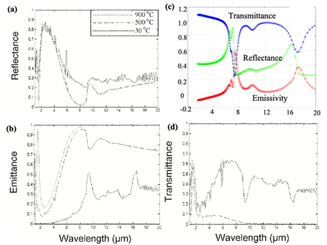
Figure 3 Comparison of optical properties of SIMOX – (a), (b), (d) measurements from the literature, at 30 oC, with simulations (c). Figure 3a, b and d are reproduced with permission from Ref.11
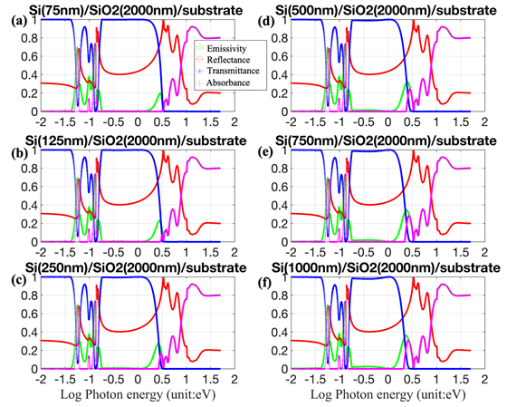
Figure 4 Emissivity, reflectance, transmittance and absorbance spectra of Si/SiO2 (2000 nm)/Si structure as a function of photon energy and thickness.
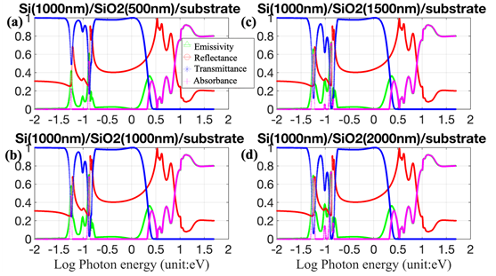
Figure 5 Emissivity, reflectance, transmittance and absorbance spectra of Si (1000nm)/SiO2/Si structure as a function of photon energy and thickness.
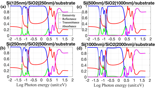
Figure 6 Emissivity, reflectance, transmittance and absorbance spectra of Si/SiO2/Si structure as a function of photon energy and thickness.
Regardless of the varying thickness of Si and SiO2, the optical properties of SOI can be categorized into three parts – based on their spectral patterns. SOI exhibits relatively complicated changes in the radiative properties in the energy range of 0.04-0.18eV. SOI exhibits 100% transmittance and ~ 40% reflectance in the energy range of 0.13-1.58eV (λ=0.78-9.85μm), and when the energy <0.04eV (λ>31μm). The Si/SiO2/Si structure shows 0% transmittance and over 90% reflectance and absorbance when the incident photon energy is >3.16eV. The thickness of the component layers has less influence in this photon energy range.
Ge-on-Si photodetectors
Fundamental optical properties of Si, Ge and SiGe alloy: In Figure 7a & 7b, n and k of Si and Ge, as a function of energy, are presented. These spectral characteristics of Si and Ge are consistent with those of Forouhi et al9 In Figure 7c, the reflectance of Si has a high value of >60% in the energy range of 3.2-5.6 eV (λ=220-400nm) (UVA to UVC). In Figure 7d, the reflectance of Ge exhibits several peaks with low reflectance in the energy range of 1- 8 eV. Moreover, the absorption coefficient of Si and Ge have similar patterns and values > 5x107 cm-1 when the photon energy is > 4eV. In Figure 8a & 8b, k of SiGe alloy shows similar dependence on wavelength to the n of SiGe. The increase in k at lower wavelengths (~ 400 nm) is due to interband absorption, and a slow variation is observed when λ is > 500 nm. In Figure 8c, the reflectance of SiGe starts with 20% for SiGe0.05; it increases to over 40% for SiGe0.15, when λ is ~ 350 nm. However, a drastic decrease in reflectance, in the UV range (λ = 400-700nm), is observed when the Ge content is increased. These optical properties are consistent with those of Kadri et al14
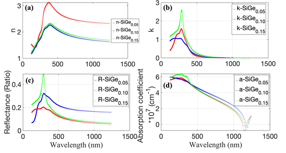
Figure 8 Simulation of optical properties of SiGe alloys - (a) n, (b) k, (b) optical reflectance and (d) absorption coefficient as a function of wavelength.
Optical properties of Si/Ge/Si structure: The results of the simulation of the optical properties of Si/Ge/Si with varying thickness are shown in Figure 9. Si/Ge/Si multilayers are transparent for photon energy <1eV and exhibit >80% absorbance when the photon energy is > 8eV. The changes in thickness of both Si and Ge have limited impact on the reflectance, emissivity, transmittance and absorbance. In Figure 9e-9h, slight changes (in 10%) in absorbance (highlighted the black circles) are observed.
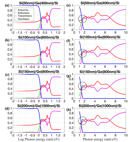
Figure 9 Emissivity, reflectance, transmittance and absorbance spectra of Si/Ge/Si structure as a function of energy and thickness.
Optical properties of Si/Ge/SOI structure: The results of the simulation of optical properties of Si/Ge/SOI, with varying thickness, are shown in Figure 10a-10d. Figure 10d shows a higher decrease in transmittance and higher increase in emissivity than the other case studies for photon energy in the range of 0.06-0.18 eV. The structure exhibits transparency for photon energy > 0.18eV. The results of the simulation of optical properties for Si/Ge/Si/SOI, with varying thickness, are shown in Figure 11a & 11b. In these figures, an increase in emissivity and a decrease in transmittance, for photon energy in the range of 0.06-0.18eV, is observed when the thickness of each of the layers is doubled.
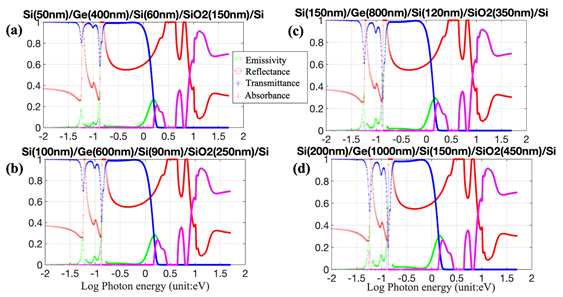
Figure 10 Emissivity, reflectance, transmittance and absorbance spectra of Si/Ge/Si/SiO2/Si structure as a function of energy and thickness.

Figure 11 Emissivity, reflectance, transmittance and absorbance spectra, based on 2016, Chong et al12 as a function of energy and thickness.
Optical properties of SiGe/Si structure: The results of the simulation of optical properties of SiGe/Si, with varying thickness, are shown in Figure 12. SiGe/Si shows almost 100% transmittance for λ >600nm when the Ge content is 0.05 and the thickness of SiGe is 100nm. The transmittance edge decreases when the Ge content is increased from 0.05 to 0.15 and the thickness of SiGe is increased from 100nm to 1100nm. The reflectance increases slightly at λ ~300nm when the Ge content is increased from 0.05 to 0.15. SiGe0.15 is more sensitive to the change in thickness compared with SiGe0.05, which exhibits almost a constant behavior in the optical properties, irrespective of the thickness. The absorbance decreases from over 90% to 0% in the wavelength range of 200-1200 nm with a slight rebound at ~ 400- 600nm; this rebound is highly sensitive to thickness, especially for SiGe0.15. The SiGe/Si multilayers exhibit constant 100% transmittance, 0% absorbance and 20% reflectance when λ is > ~ 800nm.
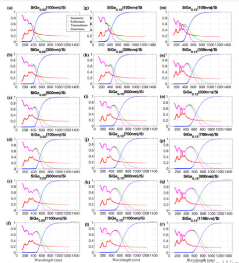
Figure 12 Emissivity, Reflectance, Transmittance and Absorbance spectra of SiGe/Si as a function of wavelength and thickness.
As a matter of general interest in materials science, it may be noted that Demir et al 17 have investigated the dispersion of the refractive index of poly(methyl methacrylate) (PMMA) and zinc oxide (zincite, ZnO) nanoparticle composites using the phenomenological Cauchy relation.17 Accordingly, they have reported the Cauchy Coefficients of the films as a function of varying ZnO content in the PMMA-ZnO composites.
In summary, this study presents a simulation of the wavelength dependence of the fundamental optical constants, the extinction coefficient and refractive index, based on the Forouhi–Bloomer dispersion equation. The simulation is applicable to the entire wavelength from radio waves to EUV spectral range. This model has been tested on various multilayers (SOI and Ge photodetector), and the results obtained are in good accord with some published data, as well as the literature. These models facilitate the calculation of the optical constants in a wide range of wavelengths. The efficacy of the proposed model is that it represents the correct picture of the optical and electronic properties depending on the structural evolution in the multilayers. Moreover, it is a well-established fact that the optoelectronic properties are susceptible to the refractive index and extinction coefficient of materials and thickness in these multilayers. Therefore, reliable data of the optical constants of semiconductors, particularly in the infrared range of wavelengths, are provided in this study. These results can be utilized for the determination and realization of the optical response, as a function of photon energy and thickness, of bulk as well as multi-layered semiconductors.
None.
The authors declare that there are no conflicts of interest.

©2020 Leqi, et al. This is an open access article distributed under the terms of the, which permits unrestricted use, distribution, and build upon your work non-commercially.