Journal of
eISSN: 2572-8466


Review Article Volume 11 Issue 5
Department of Mechanical and Biomedical Engineering, City University, Hong Kong
Correspondence: Kelvii Wei Guo, Department of Mechanical and Biomedical Engineering, City University of Hong Kong, 83 Tat Chee Avenue, Kowloon Tong, Kowloon, Hong Kong, Tel +85234424621
Received: November 01, 2024 | Published: November 6, 2024
Citation: Guo KW. Nano-porous silicon for optical interferometric biosensor. J Appl Biotechnol Bioeng. 2024;11(5):170-175. DOI: 10.15406/jabb.2024.11.00374
Since the photoluminescence was discovery at room temperature due to the quantum confinement effects, nano-porous materials have addressed intense eye-catching research focuses. The achieved results indicate that besides the superior photoluminescence, nano-porous silicon materials fabricated by the electrochemical approach are promising candidates for the utilizations in biological sensing, energy storage, chemical and catalysis, owing to the correlated biocompatibility, biodegradability, modifiable surface and high porosity, which comprise with tunable optical porous silicon structure and the applications such as biosensing, in vivo imaging, gas sensing and solar cells.
Therefore, the facile electrochemical approaches utilized to prepare nano-porous materials are addressed, particularly for nano-porous silicon materials aim to showcase the correlated significant techniques to realize green exploits for the future eco-friendly environmental developments.
Keywords: nanoporous, silicon, biosensor, etching, electrochemical, templating, bioengineering
Since the 20th century, nanotechnology has been an eye-catching hot point for scientists along with more and more huge effort putting into the relevant fields. As the same time, the technology attached with nano techniques closely to human is dramatically changed with the exploration and achievements of nanotechnology. Even for our routine life shows nanotechnology an extensively profound influence. For nano-porous materials, as a subset of nanotechnology, it is also a pivotal class with impressive utilizations for instant electrodes,1–3 sensors,4–6 catalysis,7,8 molecular separation9–12 and drug delivery, etc.13–27
It is well known that nano-porous materials correlated to biomedical applications have been significantly investigated owing to the relevant unique characteristics (such as large volume of pores, tunable size of pores, chemical stability, feasible surface modification and high specific surface area, etc.). Additionally, the structures of nano-porous materials also possess captivating fluorescent, magnetic and conducting properties. As a consequence, nano-porous materials have attractively been explored in biomedical applications, for instance, biomolecule determination, drug encapsulation, drug solubility improvement, controlled drug release, proteome analysis, targeted therapy, enzyme immobilization, gene transfer, adjuvants, tissue engineering, theranostics, regeneration medicine, nucleic acid protection, implants, fluorescent imaging, magnetic resonance imaging, electrochemical sensors, optical sensors, etc.
The highly porous nanostructure materials with the correlated pore sizes ranged from a few nanometers to one hundred nanometers are well known as nano-porous materials. In accordance with the standards of IUPAS (International Union of Pure and Applied Chemistry), three different kinds of pore can be classified according to the pore diameter (1) macropores (>50 nm); (2) mesopores, 2 nm <pore size < 50 nm; and (3) nanopores (< 2 nm). The captivating achieved results show that at the nanoscale, nano-porous materials have various fascinating properties (for instant high surface to volume area,8,28–30 plasmonic,31–34 photonic11,35,36 and quantum confinement effect,37–39 which are closely to the utilized materials.
Over the past decades, there has been a growing global emphasis on nano-porous materials for various applications. Up to now, a significant portion of investigating dedications has been put into exploring various porous materials such as metal,40–42 semi-conductor,43–46 ceramic47,48 and organic.49–51
Owing to cutting-edge synthesis strategies with significant efforts put-in, for preparing the porous materials, bulk materials can be utilized with the techniques of state-of-art. To date, pore morphologies tailored with the desired nanostructures have already successfully explored in numerous types. For the morphology of a pore, it is generally an open pore throughout to the material surface with the well-developed structures (or the tailored/desired patterns). So far, researchers have already achieved pores with various compelling structures for instant sponge-like cylinder,52–55 triangular56,57 and spherical etc.58,59 Additionally, by the electrochemical methods, other special kinds of nanostructured pores can be also obtained, such as wavy forms60 and sinusoidal forms.61
Approaches for synthesis of nano-porous materials
Etching-dealloying
As a kind of the selective etching, dealloying is a method for partial dissolution of the relevant alloy.62 It is well known that during the dealloying, etchants are always utilized to dissolve a less noble element for achieving a noble alloy left with the tailored structures in desired nano-porous. The detailed mechanism of the nanoporosity evolution during the dealloying was revealed in Nature 2001 by Erlebacher et al.63 The results express that in the dealloying, gold atoms prefer to form gold islands and are not dissolved, the pore opens up and the bulk structure continuously etches throughout. As a consequence, the sponge-like porous Au is attained after etching. Years ago, by dealloying Au/Ag, Ruffino et al.,32 obtained a type of nano-porous gold structures. The results indicate that by HNO3 dealloying, as a consequence of the volume shrinking of particles to some extent, gold crystal structure possesses the plastic deformation and lattice defects along with the shape of particles and the density of surface successfully keeping. Also, it elucidates that for the particles achieved by the liquid state process, the dealloying process is more efficient, particularly for AuAg alloy forming the particles with a more homogeneity.
Etching-electrochemical etching
It is noted that as a conventional top-down method to achieve nano-porous materials, electrochemical etching is generally utilized, where the pore is fabricated by an applied current or voltage at the bulk material electrochemically etching in electrolyte along with two or three electrode configurations using a potenetiostat in this procedure. During the processing, the electrolyte reacts with the surface of bulk materials. Consequently, the pore with the tailored structure is generated. Moreover, it should be noted that the defect sites of surface are usually the start of such reaction. The published literature relevant to nano-porous materials by the electrochemical etching has already been released: porous alumina,36,64–66 porous titania,2,67,68 porous silicon (pSi)69–71 and porous Ni.72,73
Templating method
As an approach-sacrificing a mold with target precursors filling into the relevant void space to attain porous materials, the technique-templating method was developed for applications. Actually, the electrochemical calcination or reduction is usually utilized. Up to now, as the sacrificial template, various materials can be adopted, for instant porous anodic alumina,74,75 porous silicon (pSi). Moreover, for the porous anodic alumina, owing to cylindrical pores captivating characteristics, other materials can fill into the correlated pores to successfully attain the well-defined nanotube or nanorod arrays in an easy route.76 In addition, by filling other materials into the porous silicon, for example, polymer77,78 and metal,79,80 it can achieve the photonic porous silicon with the rugated structure (particularly for the special structure).
Furthermore, as a technique of nanospheres (polystyrene or silica) application with diameter ranged from about 100 nm to 1 µm, the templating method, for instant, the nanosphere lithography81,82 is often applied. At the initial, by various approaches involved dipcoating and spincoating on the substrate, nanospheres are self-assembled to form ordered hexagonal structures. As a consequence, a monolayer or a three dimensions structure can be successfully obtained, which can be utilized as a template with different materials filling into the correlated void (for example, by the electrodeposition processing to fill the metal). In an electrolyte, metal ions are reduced to metal and filled into the nanosphere template interstices during the process of electrodeposition. After that, to achieve porous materials with the desired characteristics, the nanosphere is removed by the calcination or dissolution.
Porous Silicon (pSi)
By chemical and electrochemical etching, multidimensional and multilayers macroporous crater-like surface can be easily achieved. The attained texture with different porous morphologies is shown in Figure 1. Meanwhile, Yerokhov et al.,83 explored the relevant mathematical model of the macroporous silicon of the real layer.83
Owing to the quantum confinement effects of porous silicon (pSi), since the photoluminescence discovery at room temperature, it has significantly attracted the intense scientific research focus.84,85 Various pSi applications have been well exploited such as gas sensing, in vivo imaging and biosensing (due to the unique characteristics of tailorable surface, high porosity, biodegradability and biocompatibility) besides the photoluminescence of pSi.86 Additionally, it is significantly key to exploring pSi-based sensor for the particular optical characteristics of pSi in the reflectance spectra. To date, the modulated pSi multilayers with the waveform can be tailored into optical nanostructures (such as Bragg stacks and rugated filters) and the single layer pSi addresses Fabry-Pérot fringes.87,88
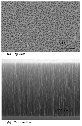
Figure 2 shows the porous silicon etched by ozone oxidization at ozone of 1.5 SCFH for 20 min in the top view and cross section. The results express that the average diameter of pores is about 37 nm in the fabricated pSi, where the attained pores are long and straight along with high porosity.

Figure 2 FESEM images-
(a) top view
(b) cross section of the porous silicon etched by ozone oxidization.
Synthesis strategies for pSi
Figure 3 depicts a typical electrochemical etching process for porous silicon achieved by crystalline silicon wafer with aqueous hydrofluoric acid (HF) connected to potentiostat. Generally, a solution of 48% aqueous HF: ethanol (3:1) is usually taken to fabricate pSi samples, where, in order to reduce the formation of bubble and improve the infiltration of etchant, ethanol is often added for increasing the wettability. The pore formation relevant to the silicon etching is addressed by Shcherban et al.,89
Si+6HF+2hole+→H2SiF6+2H++H2
Porous silicon for optical interferometric biosensor
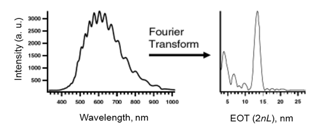
For bioengineering, particularly in field of the biological sensing, the porous silicon is a promising candidate because of the attractive tunable pore sizes with various optical nanostructures. On the basis of the optical feature of pSi (Fabry-Pérot fringes), which are the result of the peak minima and maxima of the reflection spectrum constructed by the destructive and constructive interference of the reflecting light from the bottom and the top of porous silicon layer, one of the captivating biosensors, an optical interferometric biosensor), was tailored. Figure 4 shows the Fourier transform analysis of the reflection spectrum transforms the fringes pattern to a single peak corresponding to effective optical thickness (EOT)-2nL, where n is refractive index of average porous silicon matrix and L is the optical thickness of porous silicon.

Figure 4 The Fabry-Pérot interference pattern is transformed to single peak corresponding to effective optical thickness by Fourier transform analysis.
The results express that in the refractive index of the porous silicon matrix, the alteration (induced by the binding of analytes) can be easily detected by the charge-coupled device (CCD), as the peak shift of the effective optical thickness in the reflectance spectrum, as shown in Figure 5.90–95
The porous silicon (pSi) can be quickly, effectively and easily fabricated by electrochemical approaches with tunable and controllable pore size and porosity. The attained pSi possesses the attractive optical properties which is the contribution of the large internal surface area and the versatile surface chemistry. Because of the compelling characteristics such as tunable surface, high porosity, good biodegradability and biocompatibility, nanoporous silicon materials fabricated by the electrochemical approaches are crucial to the field of biological sensing, chemical, catalysis, gas sensing, in vivo imaging and energy storage. Moreover, porous silicon is a promising candidate for optical interferometric biosensors in the coming future owing to its captivating properties. Also, it should be noted that eco-friendly techniques for pSi shall be explored further due to the chemical usage for the future environmental risks and the sustainable development.
None.
None.
Authors declare that there is no conflict of interest.

©2024 Guo. This is an open access article distributed under the terms of the, which permits unrestricted use, distribution, and build upon your work non-commercially.