MOJ
eISSN: 2577-8374


Research Article Volume 3 Issue 1
Department of Physics, Nehru Memorial College (Autonomous), India
Correspondence: Senthil Kumar S, Department of Physics, Nehru Memorial College (Autonomous), Puthanampatti, Tiruchirappalli, Tamilnadu, 621007, India
Received: July 25, 2018 | Published: March 29, 2019
Citation: Kumar SS, Rajendran A. Structural and optical analysis of electrodeposition CdZnS thin films for solar cell applications. MOJ Solar Photoen Sys.2019;3(1):30?31. DOI: 10.15406/mojsp.2019.03.00032
Investigation of CdZnS thin films were deposited on FTO glass substrate by electro deposition technique using the mixed aqueous solution of Cadmium Zinc Sulfide. The Cyclic voltammetry studies in aqueous solution were found to offer information thinfilims. The studies were performed at low pH, room temperature and fixed solution concentration, suitable deposition ranges were obtained from analysis. The deposited films we characterization by cyclicvoltammetry, (SEM) Scanning electron microscopy, when prepared in presence of capping agents.
Keywords: cadmium zinc sulfide, cyclic voltammetry, synthesis
Ternary alloy is alloy made up three different chemical elements, usually two cations and an anion and their function of composition.1 The ternary compound are found to be promising materials of optoelectronic devices applications. CdZnS thin films have been prepared variable band gap energy of 2.4 to 3.7ev widely used hetro junction solar cell and high density optical recording, blue and ultra violet laser diodes and in low voltage cathode luminescence.2 The CdZnS thin filim have prepared by variety techniques, which included evaporation spray pyrolysis, chemical bath deposition, dip techniques and organic chemical vapour deposition.3 The valuable features of the electrochemical method are the convenience for producing large area surface low temperatures growth and the possibility to control film thickness morphology composition and adjusting the electrical parameters and the compositions of electrolytes.4 The only major limitation of electro deposition is that the substrate has to be conductivity.
The depositions are carried out potentiostatically under constant deposition potentials. A regulated D.C. power source supply EG&G, MODEL 362, Princeton applied Research (potentiostat/Galvanostat) is used to prepare the CdZnS semiconductor thin film. The pre cleaned fluoride doped tin oxide (FTO) substrates were used the working electrodes. The counter and reference electrode were platinum plate and Ag/AgCl2 respectively. The distance between anode and cathode was maintained at 1cm to ensure uniform deposition. Isconnected with negative terminal to the working electrode (cathode) and the depositionof CdZnS films are achieved catholically. The required deposition potential is kept constant using potentiostat and the current during deposition was measured by an ammeter connected in series with the cathode and negative terminal of the power supply. Cathodic deposition of CdZnS films are carried out deposition potentials. The deposition of CdZnS films are carried out deposition potentials.
Electrochemical studies
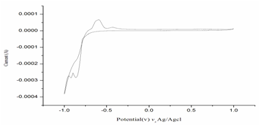
Cyclic voltammetry is a very versatile electrochemical technique, which permits to probe mechanism of redox and transport properties of a system in solution. In the present study a accomplished set up with a three electrode arrangement whereby potential relative to some reference electrode (Ag/AgCl2) at a working electrode (FTO glass plate) while the resulting current in a prepared solution like 0.001M CdCl2, 0.001M ZnCl2, 0.001M Na2S2O3 at different pH level (Figure 1).

Figure 1 Cyclic voltammogram of 0.001M CdCl2, ZnCl2 and Na2S2O3 mixture as an electrolyte with FTO glass plate (sweep rate 5mv/Sec).
The pH values were maintained by an additional of diluted HCl drop by drop. In the present study an optimization is made into prepared the solution pH at 2.5 had given two redox potential mainly -0.863mV and -0.919mV.
Scanning Electron Microscope (SEM)
Scanning Electron Microscopy technique is a promising technique for the analysis of surface texture and topography of the thin films, as it explores valuable information regarding the growth mechanism, shape and size of the particles and or grains in the thin film. In the present study Figure 2 shows the SEM image of electrodeposited CdZnS thin film at various temperature and different time respectively. From the entire prepared thin films one can understand a review of template growth phenomenon of the CdZnS thin films on the substrate for both temperature as well as different molar ratio. In Figure 2a & 2b, the SEM micrograph reveals the microstructure of polycrystalline CdS and ZnS with granular in nature). As temperature increases with at constant molar ratio and increases in deposition time, platelet like uniform structure had noticed at temperature SEM micrograph surface texture appears uniphase. This cannot be envisaged in this moment but altogether different showing strong probability of an alloy formation of CdS and ZnS with CdZnS through the prepared solution.
In the present work, CdZnS thin film has been deposited successfully using electro deposition technique in a constant reduction potential identified by cyclic voltammetry analysis. We found, the prepared CdZnS thin film exhibit Quartzite hexagonal structure and is confirmed by SEM analysis.
None.
The author declares that there is no conflict of interest.

©2019 Kumar, et al. This is an open access article distributed under the terms of the, which permits unrestricted use, distribution, and build upon your work non-commercially.