MOJ
eISSN: 2577-8374


Short Communication Volume 1 Issue 3
1Source Photonics, USA
2Source Photonics, Science-Based Industrial Park, Taiwan
Correspondence: Jack Jia-Sheng Huang, Source Photonics, 8521 Fallbrook Avenue, Suite 200, West Hills, CA 91304, USA, Tel (818) 266-7276
Received: November 03, 2017 | Published: December 21, 2017
Citation: Huang JJS, Chang HS, Jan YH (2017) Reliability challenges of nanoscale avalanche photodiodes. Open Acc J Photoen 1(3): 00015. DOI: 10.15406/mojsp.2017.01.00015
Avalanche photoiodes (APDs) are important building blocks for high-performance optical receivers. After deployment of 2.5G and 10G APD, the rapid growth of 100 GB/s Ethernet has fueled the demand of 25G APD and beyond. In this Short Communication, we briefly review the recent development of nanoscale APD and highlight the potential reliability challenges for the future.
Keywords: Avalanche photodiode, APD photodetector, 2.5G APD, 10G APD, 25G APD, InGaAs/InAlAs APD, 100Gb/s Ethernet, 100G datacenter
Solar power provides one of the key emerging renewable sources of energy for today.1 The key method to harness solar power is by means of photovoltaic effect, a phenomenon to convert light into electricity.2 In fiber optic communications, photodiode is utilized as a sensor to convert an input optical power into electrical signal by a similar photovoltaic process.3 Avalanche photodiode has been widely deployed due to its performance advantages such as high receiver sensitivity, low noise, and high bandwidth.4
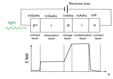
Figure 1 shows the general device schematics and electric field profile of an APD device. For the top-illumination APD illustrated in Figure 1, the top layer is a heavily p-doped InGaAs layer that forms Ohmic contact with the p-metal. The next is an intrinsic In0.53Ga0.47 as absorption layer, which has a band gap energy of 0.75eV, used to absorb light.5 To achieve lattice match to InP substrate, InAlAs is widely used for the field control and multiplication layers. The electric field reaches the maximum in the multiplication layer that is responsible for avalanche breakdown operation.4 The doping of the InAlAs field control layer can affect the relative field strength between the absorber and multiplication regions.

Figure 1 Schematic cross-section and internal electric field profile of the APD structure (not in scale). In the illustration, the InGaAs absorption layer is next to the InAlAs charge control and multiplication layers.
n.
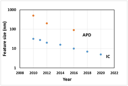
It is well known that the success of semiconductor electronics industry has been driven by the continuous feature size shrinking of integrated circuits (ICs) over the past decades.6–8 Interestingly, the photonic counterpart such as APD photodetectors is also experiencing similar miniaturization to achieve ever-increasing speed.9–11 Figure 2 shows the evolution of feature size for APD and IC since 2010. The feature size of APD refers to the thickness of the multiplication layer, while the feature size of IC is based on the length of transistor channel. It is noted that device scaling occurs for both photonic and electronic devices to attain higher performance.

Figure 2 Evolution of feature size for APD and IC. The feature size of APD refers to the thickness of the multiplication layer, while the feature size of IC is based on the length of transistor channel. Device miniaturization occurs for both photonic and electronic devices to attain higher performance.
Today, semiconductor devices often incorporate design-in reliability in the early phase.12–14 Several aspects associated with device miniaturization may impose reliability challenges. The first is the high electric field associated with feature size reduction. The increase in electric field can accelerate device degradation over long-term field use.15–17 The second factor is related to resistance and Joule heating.18–20 As device size shrinks, Joule heating is expected to increase at a given bias current. The increased Joule heating would raise device junction temperature that may excerbate functional performance and long-term reliability. The third is geometry inhomogeneity. For electronic IC, the geometry inhomogeneity may induce current crowding and cause early reliability failure.21–23 For APD, the inhomogeneous structure is typically generated by mesa etch.24–26 The etched mesa interface may cause an increase in leakage current due to the generation of surface state.24,25
Among the above three factors, increased electric field may impose the most reliability challenge for APD. This is because the effect of increased resistance and Joule heating can be mitigated by the use of mesa-type structure. For example, the resistance of the mesa-type APD is typically lowers than that of the planar-type due to the shorter conduction path.27 On the other hand, the surface leakage from mesa structure is expected to be similar from design standpoint. With careful processing control, the dark current of modern mesa-type APD devices can be confined to within a few tens of nanoamperes.5,28
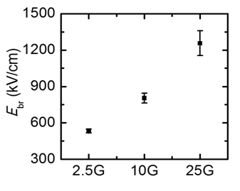
In the following, we discuss the reliability implication of increased electric field for APD. Figure 3 shows the estimated breakdown electric field in the InAlAs multiplication layer of commercial 2.5G, 10G, and 25G APDs. At the breakdown voltage for avalanche operation, majority of the voltage drop typically occurs at the absorption and multiplication layers.4 Since the absorption layer is very thick, the electric field of the absorber is usually low enough to prevent breakdown. Due to the thin layer, the electric field is much higher in the multiplication layer as illustrated in the electric field profile in Figure 1. Assuming half of the voltage drop is across the multiplication layer, we can estimate the electric breakdown field at the multiplication layer.29 It is shown that the breakdown field may reach about 800 and 1300kV/cm for 10G APD and 25G APD, respectively.

Figure 3 The breakdown electric field of the multiplication layer for various APD generations. Generally, the breakdown field increases with increasing device speed.
Although the breakdown field depends on the design of epitaxial doping and thickness,28 the ballpark estimate shown in Figure 3 suggests that reliability issue may need to be extensively studied for 25G APD and beyond. As illustrated in our recent studies,26,30,31 the two seemingly different fields of electronics and photonics share some interesting similarities in reliability physics. As device scaling continues to occur to attain higher speed and greater performance, 25G APD and beyond may mark another new frontier of reliability studies yet to be explored. With effort as relentless as IC industry, the reliability robustness of APD is expected to be achieved and matured in the forthcoming.
Nanoscale APDs are important building blocks for high-speed, high-performance optical receivers deployed in the light wave communication systems. We have reviewed the key reliability aspects associated with device miniaturization: high electric field, Joule heating, and geometry inhomogeneity. We conclude that the increase in electric field associated with device miniaturization may impose the most prominent reliability challenge for the next-generation APD.
The authors thank C.J. Ni and H.S. Chen (Source Photonics, Taiwan) for assistance in wafer processing, J.-W. Shi (National Central University, Zhongli, Taiwan) for helpful discussions, and Emin Chou (Source Photonics, Taiwan) for support of this work.
The author declares that there is no conflicts of interest.

©2017 Huang, et al. This is an open access article distributed under the terms of the, which permits unrestricted use, distribution, and build upon your work non-commercially.