eISSN: 2576-4500


Research Article Volume 4 Issue 1
1Faculty of Manufacturing Engineering, Universiti Teknikal Malaysia Melaka, Malaysia
2Faculty of Biosciences & Medical Engineering, Universiti Teknologi Malaysia, Malaysia
Correspondence: T Joseph Sahaya Anand, Faculty of Manufacturing Engineering, Universiti Teknikal Malaysia Melaka, Durian Tunggal, 76100 Melaka, Malaysia, Tel +60-6-331 6489
Received: December 30, 2019 | Published: January 20, 2020
Citation: Anand TJS, Rajan RKM, Warikh ARM, et al. Electrodeposited NiX2 (X= S, Se) thin films for solar cell applications. Aeron Aero Open Access J. 2020;4(1):1-11. DOI: 10.15406/aaoaj.2020.04.00100
Thin films of nickel chalcogenide, NiX2 (X= S, Se) have been electrosynthesized on indium-tin-oxide (ITO) coated glass substrates. The films were characterized for their structural, morphological and compositional characteristics. Their optical and semiconducting parameters were also analysed in order to determine the suitability of the thin films for photoelectrochemical (PEC) / solar cell applications. Structural analysis via X-ray diffraction (XRD) analysis reveals that the films are polycrystalline in nature. Scanning electron microscope (SEM) studies reveals that the films were adherent to the substrate with uniform and pin-hole free. Compositional analysis via energy dispersive X-ray (EDX) technique confirms the presence of Ni, S, and Se elements in the films. The optical studies show that the films are of direct bandgap. Results on the semiconductor parameters analysis of the films showed that the nature of the Mott-Schottky plots indicates that the films obtained are of p-type material.
Keywords: chalcogenides, thin films, electrochemical techniques, optical properties
Growing fuel prices and fast depleting conventional energy source has led to findings on sustainable and efficient energy source. Hence, renewable energy has been suggested as a viable approach for this particular energy crisis. Presently, many research group has focused on solar energy as the most promising renewable energy to cater the future energy demand due to its abundance and inexhaustibility.1,2
Photoelectrochemical (PEC) cell is a solar device which is fabricated with semiconductor electrolyte interface for solar energy conversion into electrical energy. Being an advance microelectronic technology, PEC can be applied for both photo voltage and chemical energy conversion.3 At present, silicon material is widely used for PEC fabrication. However, silicon is extremely expensive for large scale production.4 Thus, research is being carried out extensively in finding new materials for energy conversion for reasonable cost without compromising their conversion efficiency.5
Owing to this effort in finding new materials, Transition Metal Chalcogenides (TMC) are proposed as the most satisfactory semiconductor materials for PEC application. TMC, a combinatorial of transition metal (group 10) and chalcogenide (group 16), MX2 (M: Cd, Mo, Zn, etc.; X: S, Se and Te). TMC possesses excellent optical, electrical and semiconductor properties, especially in the thin film form.6 This advancement has motivated many researchers to investigate TMC thin film materials for PEC application namely, CdS,7 CdSe,8 ZnS,9 SnS10 etc. Cadmium chalcogenides are the most widely used TMC material for energy conversion purpose due to its significant photo conversion efficiency.8,11 However, in a recent study, Nickel has been expected to substitute Cadmium in thin film chalcogenide as a material with better electrical properties to meet solar cell expectations. It is reported that, Ni2+ has a standard ionic radius of 0.069nm, which is less than Cd2+ (0.097nm) and higher electronegativity of 1.91 Pauling compared to Cd2+ (1.61 Pauling).12 Hence, with smaller ionic radius, nickel chalcogenides could form stronger ionic bonds with higher electronegativity that makes it attract electrons effectively. Chalcogenides thin films can be fabricated by spray pyrolysis,3 electrochemical deposition,13 sputtering14 etc. One of the attractive methods for producing nickel chalcogenide thin film, owing to the possibility of large area deposition at low cost is the electrodeposition method. This method requires presence of reagents that act as a source of chalcogenide and complexion of metal ions that forms via ‘ion-by-ion growth’ mechanism.6
The first report on these nickel chalcogenides was published by Biswas.15 The results obtained shown that these chalcogenides are close to metallic behaviour due to the influence of nickel. After about two decades researchers started again on these materials but mostly focussed on chemical methods.16-18 As it is shown that nickel chalcogenides have higher electronegativity, it is proposed to study their synthesis, growth mechanism, optical and semiconducting properties of these thin films in a more systematic way. Selenium and sulphide chalcogens (X= S, Se), are non-metal while Tellurium (Te) is a metalloid. Hence, chemical behavior and reaction of sulphide and selenium is similar as compared to Telluride. The focus is given only to NiS2 and NiSe2 thin film to make comparison of the studies.
Preparation of thin film substrates and electrolytes
All reagents used for the deposition were of analytical grade. Prior to the deposition, the Indium Tin Oxide (ITO) coated glass substrates were ultrasonically cleaned in deionized water and followed by ethanol. All solutions were prepared using 30 ml of deionized water. The electrodeposition of thin film semiconductors on ITO-coated glass substrates was carried out at 40±2ºC of temperature in an aqueous solution containing Nickel Sulphate Hexahydrate, NiSO4.6H2O (1mM) + Sodium Thiosulphate Pentahydrate, Na2S2O3 (3mM) as precursors for Nickel Sulphide (NiS2) solution. Solution for NiSe2 were also prepared in the same manner except of Sodium Selenide Na2SeO3 (4mM) was used instead of Na2S2O3. Triethanolamine (TEA) (0.1M) has been added as an additive into the bath solution for successful film adhesion on the ITO-coated glass substrate.19 Besides adhesion, TEA also helps to deposit uniform and thicker deposition by controlling the deposition rate of the metal ions.19 pH of the solution was adjusted to ~ 10 by adding NaOH( 2.5mM) drop by drop6 for uniform deposition.
Characterization of electrodeposited NiX2 thin films
The electrochemical experiments, including cyclic-voltammetry (CV) and electrodeposition were controlled by Princeton Applied Research Model VersaSTAT 3 Potentiostat in a three-electrode cell, which consist of ITO-coated glass substrate as the working electrode (WE), graphite as counter electrode (CE) and Saturated Calomel Electrode (SCE) as the reference electrode (RE) as described in.6 All the three electrodes kept as close to each other with the optimum distance of 1 cm for uniform deposition.20 Film thickness of NiX2 (X=S, Se) was determined by gravimetric weight difference method using sensitive microbalance and assuming film density as close to the bulk density of the compounds.20 X-ray diffraction (XRD) and scanning election microscopy (SEM) analysis were carried out in PANalytical ZPERT PROMPD PW 3040/60 diffractometer (for 2θ range from 20 to 70° with CuKα radiation) and SEM ZEIZZ EVO 50 scanning microscope, respectively and its composition analysis with energy dispersive X-ray (EDX) analysis. Optical properties for determination of energy band gap of the films and semiconductor properties of the films studied using UV-Vis spectrophotometer and Mott-Schottky plot analysis, respectively. Mott–Schottky plots were plotted using a LCR (ZENTECH 1075- LCR at built-in frequency of 1 kHz) by adopting a two electrode configuration consisting of the thin film photo electrode and graphite as the counter electrode as illustrated in.21
Cyclic voltammetry
Cyclic voltammetry (CV) is a powerful electro analytical tool for finding redox couples and confirming the electrode potential during the film deposition process.22 Figure 1 depicts the cyclic voltammetry of NiSO4 + Na2S2O3 and NiSO4 + Na2Se2O3 solution bath.
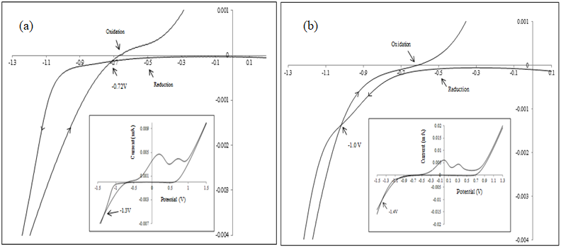
Figure 1 Cyclic voltammogram of the electrodes using ITO-coated glass substrates in alkaline solution bath of TEA and (a) NiSO4 + Na2S2O3 (b) NiSO4 + Na2Se2O3
From Figure 1 it is observed that current rise in forward scan of both NiSO4 + Na2S2O3 and NiSO4 + Na2Se2O3 solution bath occurs approximately at -0.5V followed by two large anodic peaks. Anodic peaks correspond to oxidation of nickel compound which generally emerge at positive potential region.23 As for NiSO4 + Na2S2O3 solution (Figure 1(a)), the interception between forward and reverse scan observed at -0.72V and achieved another interception at -1.30V. However, NiSO4 + Na2Se2O3 solution (Figure 1(b)), the first interception observed at -1.0V and the second interception at -1.4V. Interception of forward and reverse scan is an important phenomenon in a cyclic voltammetry due the fact, interception confirms the deposition reaction in the latter solution until all equiblirium potential is achived and completes with second interception.24 In specific, co-deposition of nickel compound occurs at this particular region. The high current output during the reduction process indicates that the presence of TEA increases the rate of deposition. Further current rise at more negative potential was due to hydrogen evolution. It is important to mention that, no stripping peaks were available in the reduction region. It coincides, nickel compound formed on the surface of the substrate does not dissolve completely into the solution containing TEA during the reverse scan.24 From Figure 1, both NiX2(X=S,Se) chalcogen observed to have similar trend of cyclic voltammetry. It could be due to the applied chalcogen (S,Se) which likely have similar chemical behaviors and reactions.
Kinetics and growth mechanism
Thin film formation of NiX2 (X=S, Se) occurs as the result of various chemical reactions taking place in the deposition bath are possibly summarized as follows: (a) the ions diffuse to the electrode surface in the electrolyte; (b) adsorbed ions are reduced at the cathode; (c) nickel, sulphide, selenium ions migrate to the reduction reaction zone and produce binary compound semiconductors22 which initiates ‘ion-by-ion’ growth. In the present investigation, ionic species of nickel, sulphide and selenide are produced by the following reaction equilibria in an aqueous alkaline deposition bath.
(1)
(ii) Chalcogenide reduction:
On the substrate surface, S2O32- reduces to sulphide:
(2)
On the substrate surface, SeO32- reduces to selenide:
(3)
Reaction (1) shows that metal ions are produces by dissociation of the metal complex while chalcogenide ions (Reaction (2) and (3)) are produced by dissociation of sulphur and selenium precursors in the aqueous alkaline medium. When the concentration of ionic species Ni2+, S2- and Se2- exceeds in the reaction bath, nucleation starts which results in growth of these thin films. The as-reduced Ni, S, and Se atoms are very active and can easily combine to produce NiX2 compound. The kinetic growth of film can be understood from the following:
(i) NiS2 formation:
(ii) NiSe2 formation:
The growth of the film was studied through the film thickness plot as shown in Figure 2. It shows an initial induction period about 10 min and thereafter, the film begins to grow. The initial induction time in the electrolyte bath is necessary for the nucleation to start on the ITO conductive glass substrate. This confirms the ‘ion-by-ion’ growth mechanism where nucleation occurs first and act as a catalyst followed by the combination of ions for the subsequent layer of thin film growth.15
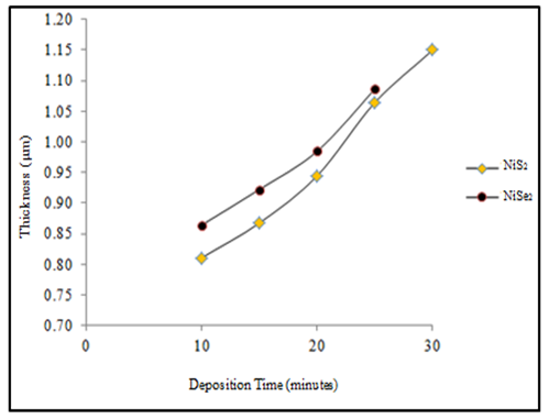
Figure 2 Variation of thickness with deposition time for NiS2 and NiSe2 thin films deposited on ITO-glass substrate.
As for 10 minutes of deposition time, the film thickness rapidly increases in the range of 0.81-0.87μm in NiX2 (X=S, Se) films. Dhanasekaran et al. has claimed that when a temperature (45°C) is applied to a solution there would be more ions available compared to room temperature.25 It is important to study that a fixed temperature of 40±2°C is applied to the solution for the influence during the deposition. Temperature plays an important role in increasing the precursor solubility and increasing the diffusion coefficient of the species and decreasing the viscosity. Thus, as soon as the deposition is started, the film thickness increases with more ions availability. Hence, it is possible for the film thickness to increase rapidly during the induction time and thereafter the thickness increase gradually as the ion diffusion become stable at constant 40±2°C throughout the deposition process. For the few cyclic voltammogram carried out it is found that As for NiS2 film, based on the CV range the deposition started to occur at -0.8 V at 15 minutes and the films display mostly amorphous nature. Improved crystallinity and film uniformity was observed at film prepared at -0.9V. However, film cracked and peeled off from ITO-coated substrate at -1.0V, 20 minutes. On the other hand, NiSe2 film growth was observed at -0.8V at 30 minutes and continued at -0.9V. Films prepared at these potentials result poorer crystallinity with less adhesion on the ITO-coated substrate. But, at -1.0V, films possess improved characterization properties. Thus, it can be understood that film distribution with good uniformity and well crystalline at potential -0.9V for NiS2 film and -1.0V for NiSe2 film was obtained.
Films were found to be well covered; with NiS2 films were in dark greyish color while NiSe2 films were in dark red as observed by the optical microscope. Film thickness increases linearly with deposition time tend to attain its maximum value at deposition time of 30 min and 25 min for NiS2 and NiSe2, respectively. There is a distinct increase in thickness of the both NiS2 film about 12% and NiSe2 10% at 25 minutes. This is close to the general trend of Se, S chalcogens thin films thickness measurement.26 It is also observed from the literature, when the film thickness exceeded the optimum value, the layers started to peel off from the substrate.27 This has been confirmed in the present investigation that, NiS2 film started to peel off from the substrate at deposition time of 35 minutes and NiSe2 peeled off at 30 minutes.
Structural characterization
Figures 3 and 4 show the XRD patterns of both NiS2 and NiSe2 film. All standard and experimental ‘d’ spacing values with reference to JCPDS cards are summarized in Table 1. This XRD analysis was performed at incident angle of 1.5º to reduce intensity of radiation reflected by the ITO glass substrate.28 It should be noted that metal substrate was not employed in this investigation corresponding to the presence of nickel which is normally detected by the metal substrate’s chemical composition. Consequently, it may lead to non-stoichiometry result in analysing NiX2 (X= S, Se) films. Undoubtedly, it is important to differentiate the XRD peaks of the substrate and the films to characterize their crystalline structure.
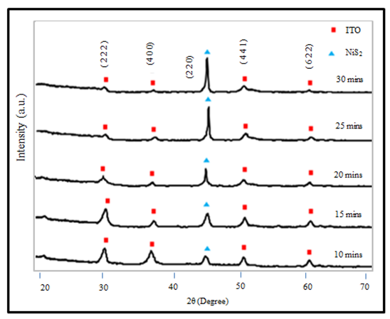
Figure 3 XRD pattern for NiS2 thin films deposited on ITO glass substrate at different deposition times.
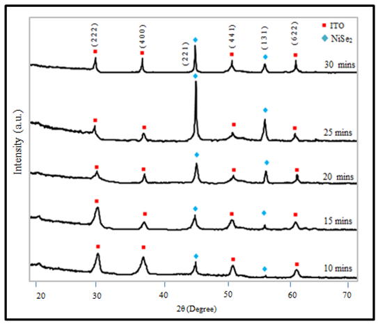
Figure 4 XRD pattern for NiSe2 thin films deposited on ITO glass substrates at different deposition times.
|
Material |
Structure |
Angle (2θ) |
Planes (h k l) |
Standard (Ǻ) |
Experimental (Ǻ) |
||||
|
‘d’ JCPDS |
10min |
15min |
20min |
25min |
30min |
||||
|
NiS2 |
Cubic |
45.547 |
2 2 0 |
1.99 |
1.9733 |
1.9544 |
1.9216 |
1.8461 |
1.7436 |
|
NiSe2 |
Orthorhombic |
47.176 |
2 2 1 |
1.925 |
1.9011 |
1.8772 |
1.8008 |
1.7745 |
1.9843 |
|
55.733 |
1 3 1 |
1.648 |
1.6302 |
1.6321 |
1.6201 |
1.5984 |
1.6272 |
||
Table 1 Comparison of experimental ‘d’ values with JCPDS data for NiX2 (X=S, Se) thin film
Peaks belonging to NiS2 film deposited for a period of 10-30 minutes is detected and labelled as shown in Figure 3. The structural features fit into the cubic structure of the NiS2 film with lattice parameter values a=b=c= 5.668nm which is in good agreement with the standard values.29 Only a single peak is attributable to NiS2 with lattice plane (2 2 0) at 2θ = 45.5º. Intensity of the peak (2 2 0) increases dramatically at 30 minutes indicating that the film grow with respect to time. From Figure 3 it is clear that the intensity of ITO peaks are initially higher for 10 minutes film which is further suppressed as the deposition time increases. This is confirmed that higher film thickness reduces the effect of substrates it utilized.
Figure 4 shows the XRD patterns of NiSe2 films and peaks emerged at 2θ = 47.48º and 55.73º that identified as (2 2 1) and (1 3 1) plane, respectively. The structural features fit into orthorhombic structure of the NiSe2 films with lattice parameter values a= 4.89, b= 5.96, c= 3.96 nm which is in good agreement with the standard values.30 At 20 minutes, hkl plane (1 3 1) started to emerge more definably that could be resulting from effective mass transfer forms a thicker film as the deposition time increases. Intensity of the plane (2 2 1) found to be more prominent than plane (1 3 1) which indicating (2 2 1) peak is the preferred orientation. However, the intensity of (2 2 1) and (1 3 1) plane shrinked at 30 minutes deposition time due to crystallinity deterioration. Crystallinity deteriorates at longer deposition time causing film to break and peel off. This result is also observed and confirmed by SEM analysis that will be discussed in section 3.3.
According to the Debye-Scherer approach,25 the interplanar distance ‘d’ corresponding to different (h k l) planes that calculated from the X-ray diffractograms. The crystallite size was calculated from the measurement of full-width at half-maximum (FWHM) in different X-ray peaks and values are in the range of 38-60 nm for NiS2 and 15-35 nm for NiSe2 which is in similar trend observed for other TMCs.31
From Figures 3 and 4, it is understand that the NiX2 (X= S, Se) has formed pure NiS2 and NiSe2 film without other phases and elements such as Ni, Ni3S2 , NiSe or other intermediary phase of both NiS2 and NiSe2 formed. The sharp and more intense diffraction peaks of these films reveals the formation of films with improved crystallinity.20 It is important to remark that, enhancement of film crystallinity achieved due to increase of film thickness and strain decrease along with increase in grain size from the polycrystalline nature of films.32 As mentioned earlier, deposition time has influence on NiX2 (X= S, Se) thin film growth since structure and grain growth of the film is mainly dependent on reaction (deposition) kinetics.
Higher deposition time shows that the decrease of the lattice constant, ‘d’ which confirms the improved crystallinity as shown in Table 1. This attributed due to decrease of Full Width Half Maximum (FWHM) with narrowing of the lines of crystal growth which indicates the grain size has increased. On the other hand, the increase of the lattice constant indicates the film peel off from substrate for films deposited more than 30 minutes. Hence, the crystallinity improvement or deterioration of the film peaks can be confirmed through the changes in lattice spacing and their corresponding lattice parameters.33
Morphological characterization of NiX2 thin films
The surface morphology of the NiX2 (X=S, Se) films obtained with different deposition times are shown in Figures 5 and 6. The deposited films were confirmed homogenous, well adherent to the substrate and uniform with the use of electron microscope. From the planar SEM of the films were investigated, it clearly shown that as the deposition time increases, the size of the crystallites and the number of aggregations in the films increased, resulting more homogeneous structure. Slow nucleation and growth rate at lower deposition time (10 minutes) causes incomplete growth in the film as it is also supported by previous XRD analysis. Thereafter, sufficient deposition time is necessary for deposition kinetics to take place in the reduction bath.
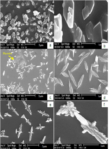
Figure 5 Planar SEM of NiS2 (a) 10min (1000X) (b) 10min (5000X (c) 20min (1000X) (d) 5000X (e) 30min (1000X) (f) (5000X).
Figure 5 shows the morphology of NiS2 film prepared for 10, 20 and 30 minutes. The formed platelet grains at the beginning of the film growth is disappeared and transformed into needle structure as the deposition time increases. At 20 minutes, a platelet grain is found among needle structures. It may be attributed to rearrangement of the film structure caused by effective mass transfer and indicating the film growth is incomplete.34 Films found to be completely in needle structure, homogeneous, smooth and evenly distributed at deposition time of 30 minutes. Additionally, number of aggregations in the film found to have increased due to denser film at the latter deposition time.35 Similar observation of that needle like crystallites provide direct pathway for the transport of the photogenerated carriers and mobility of carriers in such microstructure is higher resultant of less number of intergrain boundaries.34 The variation of the calculated average platelet grain size is in the range of 0.61-0.70μm. However, the needle like grains are in the average length of 2.72-4.36μm and diameter of 0.12-1.23μm.
On the other hand, the morphology of the NiSe2 film is found to be well defined in spherical shape. Few crystallites are grouped together forming larger grains. It could be of the effect of Ostwald ripening process as Se elemental is reported to have amorphous structure in alkaline bath and often aggregates to form spherical morphology.36 The calculated grain size found to be in the range of 0.12-0.39μm. Additionally, the films are found to be continuous, well covered, homogenous and without voids up to 25 minutes, thereafter, film started to crack and peel off. Longer deposition time bring the effect of the growth of the particles with constant temperature.37 This explains that longer the deposition time does not promise better film morphology. As the size of the grains increase corresponding with increasing deposition time, the film become thicker and strain energy increases. Consequently, the film cracks to release the stress accumulated.38
It is observed that, the morphology of the structure is smoother for films with sulphur content as compared to its NiSe2 counterpart. Theoretical calculation of grain size is slightly varied with the actual experimental morphology as the grain growth is influenced by preparation method and its parameters. It should be noted that, all grain size of the film is larger than 1μm. Chui et al.,42 claims that larger grain size (>1μm) could increase energy conversion of solar cell of an absorber material. Hence, the prepared NiX2 (X= S, Se) thin films can be considered as one of the suitable materials for the application in solar cell.
Compositional characterization by EDX analysis
As shown in Figure 7, Energy Dispersive X-ray (EDX) was used to analyse the film stoichiometry of the prepared samples of 30 and 25 minutes for NiS2 and NiSe2 respectively. These samples are considered to be the optimum films for revealing their stoichiometry. The strong peaks in the spectra for Ni, S, and Se were identified and are near stoichiometric with ratio close to 1:2 as presented in Table 2. Although elements of C and O do not have any influential role in the synthesis of the films, their peaks also observed in the spectrum corresponding to the capability of EDX to detect as low atomic number elements such as carbon and oxygen, which is ubiquitous in our environment. Inclusion of oxygen is found in all the films because it is found to be unavoidable for chemically deposited films as testified. This is true and accepted for all films synthesized.6 Furthermore, the spectrums also display smaller peaks of Na, which has been expected as Na was used as a precursor in the electrolyte for the deposition of films.
|
Material |
Atomic weight % |
Atomic ratio |
|
NiS2 |
32.74 : 64.33 |
NiS1.96 |
|
NiSe2 |
31.48: 62.45 |
NiSe1.98 |
Table 2 Compositional study of NiX2(X=S,Se) excluding other constituents
Optical properties of electrodeposited thin films
The optical absorption spectra of NiX2 (X=S, Se) thin films deposited onto ITO glass substrate was studied in the wavelength range 200-1100nm without considering losses due to reflection and transmission. Optical behavior of a material is vital for photoelectrochemical application and generally utilized to determine its optical constants, i.e. absorption coefficient (a), extinction coefficient (k), optical band gap (Eg) etc.40 For this purpose, absorbance data, amount of light absorbed by the sample are taken.
From the optical absorbance versus wavelength data, band gap energy and band transition type was derived from mathematical treatment of the data with the following relationship for near-edge absorption.41
(4)
where u is the frequency, h is the Planck’s constant, C is velocity of light, is the wavelength, k equals a constant while n carries the value of either 1 or 4. Tauc’s plot has employed to plot the (αhu)1/2 graph. According to42 Tauc’s plot is the plotting of (αhu)1/2 as a function of photon energy (hu) for different values of n (n=1 and 4).24 It ensures the direct and it’s allowed transmissions in the material if a straight line is obtained for n= 1, it indicates a direct electron transition between the states of the semiconductor, whereas, the transition is indirect is a straight line graph is obtained for n=4. The straight line intercepts to the energy axis yields the optical band gap.31 The graph of (αhu)2 versus photon energy is shown in Figure 8(a) and the related Eg vs deposition time is plotted in Figure 8(b).
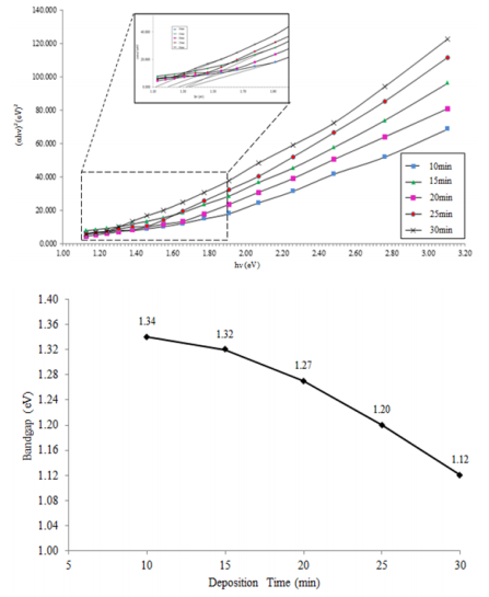
Figure 8 Variation of NiS2 thin films deposited at different deposition times. (a) (αhʋ)2 vs.hv and (b) bandgap vs. deposition time.
From the Figure 8, it can be understand that the band gap range for NiS2 film prepared at various deposition time is in the range of 1.34-1.12 eV. The obtained band gap range is in good agreement with the value reported.41,43 Similar observation shown in Figures 9(a) and 9(b) of the band gap range for NiSe2 film prepared at various deposition times is in the range of 1.30-1.15eV. The obtained band gap range is in good agreement with the value reported.44,45
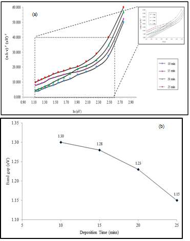
Figure 9 Variation of NiSe2 thin films deposited at different deposition times. (a) (αhʋ)2 vs. hʋ and (b) bandgap vs. deposition time.
These NiX2 films optical band gap value is in the decrement trend that fits into the trend of thin film band gap values. It is observed that the values of these chalcogens are within the close range. It can be concluded that the optical bandgap energy of all types of films decreases as the deposition time of the film increases. This result correlates to film thickness, whereby an increase in deposition time of the films result in higher thickness which correlated as film thickness increases with respect to the amount of light energy.46 When the deposition conditions like substrate temperature of the film and solution concentration are kept fixed, the value of the band gap in general changes according to the thickness. According to Guneri et al.,35 the reasons for this change can be one of the following: (i) largeness of the dislocation, (ii) quantum size effect (not relevant for thin film studies), (iii) changing barrier height due to variation in grain size in the polycrystalline film. As it is evident that the band gap is affected by causing an alteration in the values of these band gap of the deposited films and decrease in barrier height is caused by an increase in grain size which in turn caused by an increase in film thickness. The decrease in energy band gap after long periods of deposition time is also attributed by improved crystallinity with sufficient thickness as supported by an increase in film thickness. The corresponding values of the band gap energy of the films with respect to film thickness are given in Table 3, is also reported that band gap decrease due to reduced Urbach energy in the optical band with increased film thickness. It is a good sign indicating decrease of defects in the film which is correlated to the disorder in the film.32
|
Deposition Time (min) |
NiS2 |
NiSe2 |
||
|
Film Thickness (μm) |
Bandgap (eV) |
Film Thickness (μm) |
Bandgap (eV) |
|
|
10 |
0.8105 |
1.34 |
0.8641 |
1.3 |
|
15 |
0.8674 |
1.32 |
0.9222 |
1.28 |
|
20 |
0.9444 |
1.27 |
0.9846 |
1.23 |
|
25 |
1.0642 |
1.2 |
1.0864 |
1.15 |
|
30 |
1.1498 |
1.12 |
Film peeled OFF |
|
Table 3 Bandgap energy values corresponding to film thickness of NiS2 and NiSe2 thin films
Overall, the time dependent parameters that effect the band gap are expected due to reorganization of the film and self-oxidation of the film which is apparent in SEM studies. By filling the voids in the film as the deposition time increases, denser films and smaller energy gap is expected.
Semiconductor parameters of electrodeposited thin film
Space charge capacitance (Csc) is vital parameter to characterize a semiconductor-electrolyte interface. The measurement of space charge capacitance plays a pivotal role in understanding the type of conductivity, flat band potential (VFB) and depletion layer width due to the purpose to identify the semiconductor characteristics of these thin films that would be suitable to be utilized as PEC cell materials.34 The measurement of space charge layer capacitance as a function of applied potential under depletion condition is based on Mott-Schottky relationship6:
(5)
where Csc is the capacitance of the space charge region, ε and ε0 are the dielectric constant of semiconductor and permittivity of free space respectively, N is the carrier concentration which is calculated from the slope of the graph and V, Vfb are the applied and flat band potentials, respectively.
The dielectric constants, ε for the films have been determined by the relation [6]:
(6)
Where C is the capacitance, d is the thickness of the film and A is the area of contact (2.23 x 10⁻⁶ m2). The band bending (Vb) is another important parameters which can be calculated from the relation:
(7)
Where VF,redox is the redox potential of the film electrolyte. VF, redox is deduced as:
(8)
However, since two electrodes configuration consisting thin film photoelectrode and graphite as counter electrode is adopted for the Mott’s measurement [21], Vsce(Ag/AgCl) value is not included in the semiconductor parameter studies. Hence, the VF,redox can be deduced as :-
(9)
VF,redox equal to the applied potential -0.9V and -1.0V for NiS2 and NiSe2 thin films respectively.
Equation below represents depletion layer width [6]:
(10)
An expression for the density states, Nc can be written as[6] :
(11)
where h is Planck’s constant (4.136 x 10⁻¹⁵ eVs) , me* is the effective electron mass in the conduction band and taken as ≈ 2.5 me*.47
Under constant illumination, maximum efficiency is given by:6
(12)
Conversion efficiency varies for different materials. Thus, this theoretical efficiency calculation is necessary to get overview of the material efficiency before doing modification in the fabrication. Conversion efficiency most likely corresponding to the following factors:34
High conversion efficiency is the immense requirement in PEC fabrication. From the expression (12) it is clear that maximum efficiency depends upon band bending (Vb) and band gap (Eg). Larger the band bending, the higher would be the photoconversion efficiency which is the pivotal requirement for PEC application.
Bend bending occurs at the interface between the semiconductor photocathode and the electrolyte which is resultant from “solid-electrolyte” phenomena. The space charged region is formed at the interface. This space charge region provides the electrical field strength that is responsible for an effective separation of photo excited electrons from holes. Since Fermi level occupy carriers, the band move towards the Fermi layer. This is evident that band bending is influenced by the position of the Fermi level.48 In a p-type material, the fermi level is close to valence band and making the band bend downwards.49 Hence, it can be said that band bending gives maximum possible output photovoltage from the semiconductor device.
The Mott-Schottky plot of NiX2(X=S,Se) thin films is shown in Figures 10 and 11 and their corresponding semiconductor parameters summarized in Tables 4 & 5, respectively. Intercepts of plots on voltage axis determine the flat band potential value of the material. Flat band VFB, potential forms when the band bending of the material is affected by the external voltage, in no space charge layer.48 Flat band provides information on charge transfer process across the semiconductor-electrolyte junction of PEC cell. Figure 10 shows the Mott-Schottky plot for NiS2 thin films at different deposition time. The values of semiconductor parameters obtained for the films are shown in Table 4. The flat band potential (VFB) value is observed to increase from 1.00 to 1.48V as the deposition time increases.
|
Semiconductor parameters |
NiS2 thin film |
||||
|
10min |
15min |
20min |
25min |
30min |
|
|
Type of semiconductor |
p |
p |
p |
p |
p |
|
Flat band potential (VFB) (V) |
1 |
1.22 |
1.31 |
1.37 |
1.48 |
|
Dielectric constant, (ε) x (1028) |
2.09 |
2.81 |
3.62 |
4.85 |
6.13 |
|
Acceptor density (NA) x 1029 ( m-3) |
-1.96 |
-2.14 |
-3.12 |
-4.61 |
-5.95 |
|
Depletion layer width (W) x 10-3 (Ǻ) |
-2.88 |
-3.66 |
-4.18 |
-4.93 |
-5.04 |
|
Density of states in conduction band (Nc) x 1013 (m-3) |
1.518 |
1.518 |
1.518 |
1.518 |
1.518 |
|
Band bending (Vb) (V) |
-1.9 |
-2.12 |
-2.21 |
-2.27 |
-2.38 |
|
Energy gap (Eg) (eV) |
1.34 |
1.32 |
1.28 |
1.22 |
1.14 |
Table 4 Summary of the results obtained from the Mott-Schottky plots for NiS2 films
Figure 11 shows the Mott-Schottky plot for NiSe2 thin films at different deposition time. Also, flat band potential, VFB of NiSe2 increased. The values of semiconductor parameters obtained for the films are shown in Table 5.
|
Semiconductor parameters |
NiSe2 thin film |
|||
|
10min |
15min |
20min |
25min |
|
|
Type of semiconductor |
p |
p |
p |
p |
|
Flat band potential (VFB) (V) |
1.5 |
1.54 |
1.64 |
1.68 |
|
Dielectric constant, (ε) x (1028) |
2.23 |
2.61 |
3.35 |
4.02 |
|
Acceptor density (NA) x 1029 ( m-3) |
-1.45 |
-3.07 |
-3.23 |
-3.75 |
|
Depletion layer width (W) x 10-3 (Ǻ) |
-3.42 |
-4.51 |
-5.81 |
-6.15 |
|
Density of states in conduction band (Nc) x 1013 (m-3) |
1.518 |
1.518 |
1.518 |
1.518 |
|
Band bending (Vb) (V) |
-2.5 |
-2.54 |
-2.64 |
-2.68 |
|
Energy gap (Eg) (eV) |
1.28 |
1.26 |
1.22 |
1.16 |
Table 5 Summary of the results obtained from the Mott-Schottky plots for NiSe2 films
Based on the semiconductor parameter studies, it is understood that NiS2 possess better energy conversion efficiency than NiSe2. NiSe2 is a good paramagnetic metal while NiS2 is Mott insulator.50 On the other hand, the value of flat band potential,VFB, depletion layer width, W and band bending,Vb for all films found to increase in thicker films. Flat band potential increases correspondingly with band bending as the fermi level shifts upward direction with increase carrier in thicker films.3 Depletion layer width reported to increase in a forward biasing, whereby the carrier migration is by majority carriers. In the present study, doping density (N), depletion layer width (W) and band bending (Vb) of all films found to be negative. P-type semiconductors are negatively charged and known as cathode due to filled with negatively charged acceptor ions.51,52 Departure of an electron from the N-side to the P-side leaves positive donor ion on the N-side while the hole leaves a negative acceptor ions on the P-side. Hence, the mentioned semiconductor properties of all films in p-type material are in negative value. It can be summarized that the incremental changes in semiconductor parameters can be related to the modification in the photocathode (thin film) properties namely increased photoelectrode absorption, decreased band gap and improved grain structure etc.3 With the compilation of the results on the semiconductor parameters, a comparison study was done to evaluate the suitability of the NiX2 (X=S,Se) thin films as a solar/PEC cell material. All values come in the range of many other transition metal chalcogenides and this has proven that NiX2 (X=S,Se) thin films capable as a solar / PEC cell material.
Results proved that NiX2 (X=S,Se) thin films were successfully deposited on ITO-coated glass substrates. All films obtained were well adherent to the substrate with the help of TEA by adopting ‘ion-by-ion’ growth mechanism. XRD analysis of the films proved NiX2 (X=S,Se) thin films is polycrystalline while EDX pattern confirmed the Nickle(Ni), Sulphide (S) and Selenium(S) element presents in the thin film formed through electrodeposition process. Electron microscope analysis confirmed the uniform and smooth nature of the films. Optical studies show the direct optical bandgap energy of the film. Results on the semiconductor parameters of the films revealed it is of p-type material and all semiconductor values come in the range of many other transition metal chalcogenides and this has proven that NiX2(X=S,Se) thin films is capable as a solar/PEC cell material.
The work presented in this manuscript was supported by the Ministry of Higher Education (MoHE), sponsored by KeTTHA / FRGS grant (Project No. FRGS/2011/FKP/TK02/1 F00120) and Universiti Teknikal Malaysia Melaka (UTeM).
Authors declare that there is no conflict of interest.

©2020 Anand, et al. This is an open access article distributed under the terms of the, which permits unrestricted use, distribution, and build upon your work non-commercially.