eISSN: 2576-4543


Research Article Volume 4 Issue 5
Andijan State University named after Babur, Uzbekistan
Correspondence: R Aliev, Andijan State University named after Babur, 129, University st., Andijan, 170100, Uzbekistan, Tel (374) 223-83-71, Fax (374) 223-88-30
Received: October 10, 2020 | Published: October 22, 2020
Citation: Aliev R, Abduvohidov M, Gulomov J. Simulation of temperatures influence to photoelectric properties of silicon solar cells. Phys Astron Int J. 2020;4(5):177-180. DOI: 10.15406/paij.2020.04.00219
The method of digital modeling investigates influence of temperature on photoelectric processes in silicon solar cells. Feature of program system describes “Sentaurus TCAD” which is allowed to model silicon solar cells with flat p-n-junction. Results of research are received in the form of visual pictures of processing of volume of silicon with p-n-junction, processes of photogeneration of nonequilibrium carriers of a charge at illumination and thermal emissions at the account of various mechanisms of their recombination, and loading of I-V characteristic of solar cell at various temperatures. Results of estimation temperature factors of a current of short circuit Jsc, open circuit voltage Uoc, fill factor of I‑V FF, the maximum power Pm and efficiency ŋ for silicon solar cells without and with nanoparticles of metal are compared. It is noticed that despite high values of the basic photoelectric parameters of the solar cells containing nanoparticles of metal, than without them, temperature factors of target power and efficiency worsen a little. Means, in such cases acceptance of measures for cooling of solar cells is required. On the other hand, higher photosensitivity of plasmon solar cells is shown at low temperatures. There is a perspective possibility of creation high-sensitivity (plasmon) photosensors for a special purpose, working at low temperatures.
Keywords: photovoltaic, silicon, solar cell, simulation, temperature
The most promising and environmentally friendly type of renewable energy sources is photovoltaic converted solar energy. The efficiency of photovoltaic power devices is primarily determined by the efficiency of semiconductor photovoltaic energy converters. More than 85% of the semiconductor solar cells (SCs) are made from silicon.1 The efficiency or performance of silicon SCs directly depends on the level of illumination and ambient temperature.2 In order to generate more photovoltaic energy from each SC, an increase in the level of their illumination is required by concentrating solar radiation from a large area of the concentrator onto a small surface of the SC.3 This method makes it possible to reduce the area of expensive silicon SCs used. However, at the same time, a significant increase in the temperature of SCs consequently decrease their efficiency. Therefore, in systems with concentrators, the use of SCs made on the basis of gallium arsenide compounds, which have more stable parameters at higher temperatures than silicon SCs, is practiced.4 However, SCs based on gallium arsenide compounds are almost an order of magnitude more expensive than silicon ones. In this regard, it is considered expedient to use such SCs in systems with concentrators only for the needs of the space industry. For the needs of ground-based energy, it is recommended to use silicon SCs. In regions with hot climates (high temperatures), it becomes a problem to use silicon SCs even without radiation concentrators. The development of technical measures for cooling silicon SCs is complicated by the fact that the temperature coefficients of the main photoelectric parameters differ significantly from each other depending on the type of silicon base material, the quality of the p-n junction, the stability of the contact electrodes, and the quality of antireflection coatings (ARC). In addition, when creating SCs of the second and third generation, surface and volumetric innovative (technical solutions) optical traps are used, which can significantly affect the temperature coefficients of the main photoelectric parameters of such SCs.5,6 For example, in structures of the third generation SCs, nanoparticles of various metals are implanted into the near-surface layers of silicon in order to realize the effect of nanoplasmonics.7 Therefore, it becomes urgent to study the effect of temperature on the main photoelectric parameters of thin silicon SCs containing metal nanoparticles in the bulk or in the near-surface layer. The present work is devoted to this urgent task.
The method of digital modeling of processes of photoelectric generation of nonequilibrium charge carriers and their transfer in silicon SCs with p-n junction is chosen as the main research method in the presented work. There are various modeling methods for the digital modeling of semiconductor SCs. In particular in8 a statistical model of the operation of a silicon solar battery under the influence of the main environmental factors (solar radiation, humidity, temperature, wind speed) is proposed, which makes it possible to predict the generated power of a solar battery with an accuracy of 5%.9 In the methods of mathematical analysis, subject-logical and structural-functional analysis, the Design Lab and Matlab Simulink modeling software packages were used. Also of great importance of the technology is creating a database of solar power plants, proposed in.10 The selected research method of digital modeling in the form of a licensed software system "Sentaurus TCAD" is the newest and most powerful capabilities.11,12 First of all, let us note some features of the chosen software system. Sentaurus is a TCAD toolkit that simulates the fabrication, operation, and reliability of microelectronic and nanoelectronic semiconductor devices. Sentaurus is based on the use of physical models to represent the stages of wafer fabrication and device operation, which allows not only to study, but also to optimize designs (shapes and sizes) and parameters of new semiconductor devices. The Sentaurus TCAD system has numerous working software packages with wide functionality. The study used packages such as SDE, Sentaurus Device, SVisual packages and the Sentaurus Workbench infrastructure to describe the effect of temperature on the main photovoltaic parameters of silicon SCs.
The complex of devices of the Sentaurus TCAD system made it possible to calculate the rate of optical generation of charge carriers at different temperatures in an illuminated SC and connect them with the process of modeling the electro physical characteristics. Using Sentaurus Device, several methods have been implemented to calculate the rate of generation of optical signals. In addition, a thermodynamic model was used to calculate the effect of temperature on the parameters of a silicon SC. In the study of the temperature properties of silicon SCs, the temperature range of 250÷350 K is considered, which is the great practical importance for ground and space applications. The choice of the upper limit of the temperature rise of the SCs of 350 K is because at higher temperatures, the efficiency of the SCs significantly decreases and their use without cooling systems becomes impractical. The choice of the lower limit of the temperature of SCs 250 K is because during their operation in space, for example, as a power source for artificial earth satellites, it is allowed to reduce the temperature of the SC (in the absence of direct illumination by the sun) to the specified value.14
The results of the study were obtained in the form of visual pictures of processing a volume of silicon with a p-n-junction, processes of photogeneration of nonequilibrium charge carriers under illumination and heat release taking into account various mechanisms of their recombination, as well as load current-voltage characteristics of SCs at different temperatures. When a photon with an energy exceeding the silicon band gap is absorbed, photogeneration of electron-hole pairs of charge carriers occurs due to the transition of covalently bound electrons to the conduction band. After their lifetime, free electrons undergo (nonradiative) recombination, during which the main (recombination) heat release occurs. Naturally, processes of Joule's heat, Thomson's heat and Peltier heat take place in the crystal. In Figure 1 shows the load current-voltage characteristics of silicon SCs at various temperatures in the range of 250–350 K. Earlier studies of the authors of this work have investigated the processes of photoelectric energy conversion in silicon SCs.15 Some features of photoelectric processes of charge transfer in thin silicon structures with a p-n junction containing nanoparticles of various metals with different sizes and density of their distribution were established by the method of digital modeling. The most effective absorption of the solar radiation spectrum in the region of the emitter up to the metallurgical boundary of the pn-junction and the best efficiency of photoelectric energy conversion of silicon SCs with such a structure were revealed. The optimal sizes of metal nanoparticles, the regularities of their distribution, the depth of the pn-junction for thin layers of crystalline silicon have been determined.
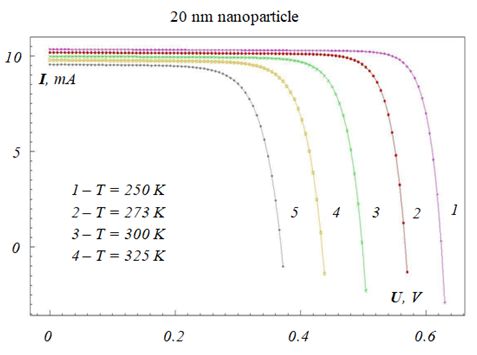
Therefore, in this work, we have determined the load current-voltage characteristics of silicon SCs, into the emitter layer of which spherical metal nanoparticles with a radius of 20 nm are embedded at different temperatures in the above range. The course of changes in the type of load current-voltage characteristics of silicon SCs containing spherical metal nanoparticles with a radius of 20 nm in the emitter layer with temperature are shown in Figure 2. If we analyze the I-V characteristics of silicon SCs obtained for temperatures, one can see not only the change in the short-circuit current Isc and the open circuit voltage Uoc, but also the fill factor of the I-V characteristic FF, the maximum power Pm and the efficiency ŋ. The results of evaluating the temperature coefficients of the short-circuit current Isc and the open-circuit voltage Uoc, the filling factor of the I - V characteristic FF, the maximum power Pm and the efficiency ŋ for silicon SCs without and with metal nanoparticles are shown in Table 1. Comparison of the temperature coefficients of the main photoelectric parameters of silicon structures determined in this work with the data of experimental works2,16 indicates their satisfactory agreement. It should be noted that the temperature coefficients of the main photoelectric parameters of silicon structures containing metal nanoparticles dVoc/dt, dJsc/dt, dFF/dt, dP/dt and dŋ/dt were determined for the first time. As is known, for silicon SCs, the effect of temperature on the current density of the SC. Insignificantly.2,16 However, the results obtained in this work indicate that the presence of metal nanoparticles in the bulk of the silicon crystal causes a significant increase in the value (more than one order of magnitude) dJsc/dt=0,0079 mA/cm2 оC, and this dependence is a linear function. This difference, apparently, is associated with the nature of the change in the photoconductivity of silicon due to an increase with temperature in the rate of thermionic emission of electrons from metal nanoparticles. A more refined conclusion can be obtained by a detailed analysis of the effect of temperature on the work function of the metal, the photoconductivity of silicon, the mobility of the nanoparticles and etc.

Figure 2 Loading I-V characteristic of silicon solar cell, containing in emitter layer with regular intervals distributed nanoparticles of metals (Pt) the spherical form with radius 20 nm.
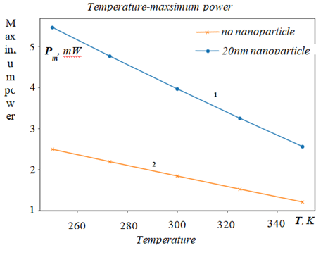
According to Table 1, it can also be noted that metal nanoparticles do not affect the temperature coefficient of the open circuit voltage. It can be assumed that, due to the presence of metal nanoparticles, the nature of the change in the band gap of silicon with temperature remains unchanged. This conclusion is also confirmed by the results of measuring the spectral characteristics of structures at different temperatures (such characteristics are not given in the article). The analysis of the rate of change of the maximum output power of silicon SCs depending on their temperature is carried out. In Figure 3 shows the curves of the calculated dependence of the temperature coefficient of the maximum power dPm/dt on the temperature of the SC formed on the basis of crystalline silicon with and without metal nanoparticles (1–Si(Pt); 2–Si). The value for dPm/dt is for silicon with and without metal nanoparticles (1–Si(Pt); 2–Si), respectively, 0,0290 mW/cm2 оC and 0,0128 0,0290 mW/cm2 оC. The relatively high value of dPm/dt (almost 2.3 times) for SC made of silicon containing metal nanoparticles is associated with a rapid rate of decrease in the photocurrent density of the short circuit with increasing temperature (Table 1). In Figure 4 shows the graphs of the maximum power of a silicon SC at T=250 K da depending on the photovoltaic voltage for cases of using crystalline silicon with and without metal nanoparticles (1–Si(Pt); 2–Si).

Figure 3 Change of the maximum power of a silicon SCs in depending on Photo-voltage: 1 - Si (Pt); 2 - Si.

Figure 4 Change of the maximum power of a silicon SCs at Т=250 K in depending on Photo-voltage: 1 - Si (Pt); 2 - Si.
Material features |
Temperature coefficients of solar cell parameters |
||||
dVoc /dt |
dJsc /dt |
dFF/dt |
dPm/dt |
dŋ/dt |
|
(mV / оC) |
(mA / sm2 оC) |
(1 / оC) |
(mW/sm2 оC) |
(1 / оC) |
|
Si |
2,56 |
0,00067 |
0,0012 |
0,0128 |
0,0128 |
Si (Pt) |
2,56 |
0,0079 |
0,0012 |
0,0290 |
0,0290 |
Table 1 Temperature factors of the main photoelectric parameters of SCs on the basis of silicon without and with platinum nanoparticles
A significant difference in the values of Рm (Т) and Рm (U) SCs formed on the basis of crystalline silicon with and without metal nanoparticles (1-Si (Pt); 2-Si), clearly distinguished in Figure 3 and Figure 4, apparently, is associated with the contribution of the effect of nanoplasmonics, realized due to the local plasmon resonance of the frequencies of oscillations of the electron density around metal nanoparticles.15 On the other hand, the contribution of the nanoplasmonic effect to the increase in the SC photocurrent becomes more pronounced at low temperatures. Apparently, at low temperatures, recombination processes in the space charge region of the p-n junction are minimized due to the transition from the region of intrinsic base conductivity with a concentration пi to impurity conductivity пр. In this case, it is necessary to take into account the temperature dependence of the concentration of intrinsic charge carriers:13
Therefore, from the results, it can be concluded that with the introduction of metal nanoparticles with certain geometric dimensions and distribution into the structure, the photoelectric parameters of the SC are significantly improved. However, at the same time, there is some deterioration in the temperature coefficients of some basic photovoltaic parameters of the SC. In other words, when operating a SC with metal nanoparticles, it is necessary to take measures to prevent their overheating.
Thus, in conclusion, the following points can be noted. First, despite the relatively high values of the main photovoltaic parameters of SCs containing metal nanoparticles than SCs, without them temperature coefficients of output power and efficiency are somewhat worse. Therefore, in such cases, special measures are required to cool the SCs. Second, the higher photosensitivity of plasmonic SCs manifests itself at low temperatures. It can be assumed that there is a promising possibility of creating highly sensitive (plasmonic) photosensors for special purposes operating at low temperatures.
None.
The author declares there is no conflict of interest.

©2020 Aliev, et al. This is an open access article distributed under the terms of the, which permits unrestricted use, distribution, and build upon your work non-commercially.