eISSN: 2576-4543


Research Article Volume 2 Issue 3
Faculty of Education, Gunma University, Japan
Correspondence: Yuki Aoki, Faculty of Education, Gunma University, Maebashi 371?8510, Japan, Tel 8127?2207 293
Received: November 24, 2017 | Published: June 7, 2018
Citation: Aoki Y. Lattice spacing distribution at Pd/Ag(111) interface by transmission electron microscopy. Phys Astron Int J. 2018;2(3):213-216. DOI: 10.15406/paij.2018.02.00088
The Pd/Ag interface structure was investigated by transmission electron microscope (TEM) and reflection high–energy electron diffraction (RHEED). The Pd was deposited on the Ag(111) surface at room temperature. The surface lattice spacing change during the Pd growth was investigated by RHEED. Cross–sectional TEM was used to examine the lattice spacing distribution across the Pd/Ag interface in the in–plane and the out–of–plane directions, separately. The in–plane lattice spacing distribution observed by RHEED and TEM measurements are quantitatively consistent, and the lattice spacing was drastically reduced from the intrinsic Ag crystal to Pd crystal one within 10 monolayer thin region. From the comparison with the out–of–plane lattice spacing distribution, the lattice near the Pd/Ag interface was found to isotopically expand.
Our results indicate that the Pd/Ag interface is sharply changed from the intrinsic Ag(111) to Pd(111) within 10 monolayer intermixing region.
Keywords: palladium, silver, interface, transmission electron microscopy, reflection high–energy electron diffraction
Pd, Palladium; Ag, Silver; TEM, transmission electron microscope; RHEED, reflection high–energy electron diffraction
The Pd–Ag is one of the most studied alloy systems, showing to form continuous solid solutions over large range of temperatures and compositions in the bulk system.1 Pd and Ag atoms are fully miscible and usually to form of fcc structure in equilibrium, except several possible ordered structures at the specific compositions, such as Pd0.75Ag0.25, Pd0.5Ag0.5, and Pd0.25Ag0.75.2 Since the pure Ag crystal has a 5% larger lattice constant than the Pd one, the lattice spacing of the alloy gradually changes from the Pd to Ag one with Ag concentration.3
The alloying mechanism at the surface is not directly related to the alloying in bulk, due to the kinetically limited processes (nucleation, diffusion, segregation etc.). The annealing causes the Ag atoms segregation to the surface,4–6 and an Ag high concentration close to 90% is often reported at the surface.7–10 High Ag concentrated surface has the lattice spacing of the intrinsic Ag one.
The intermixing between two components is disturbed under room temperature condition. Pd growth at room temperature on the Ag (111) has been investigated by Auger electron spectroscopy5 and X–ray diffraction.11 The Ag segregation was observed when the annealing temperature exceeded of ∼500 K. So far, Pd and Ag have been regarded as interdiffusion–free at room temperature deposition, and the Pd/Ag interface is atomically distinguishable.
In the lattice spacing viewpoint at the Pd/Ag interface, how–ever, the lattice spacing was not drastically changed across the interface, but was slowly relaxed from Ag to Pd lattice spacing with a long–range distribution at room temperature deposition. The surface Pd atom lattice spacing during the Pd(111) growth on the Ag(111) surface has been reported by the diffraction spot length of a reflection high–energy diffraction (RHEED) pattern.5 The surface Pd lattice spacing was expanded to the Ag crystal one when the Pd film thickness ( ) was small, and then relaxed to the intrinsic Pd crystal one at ∼100 monolayer (ML). By RHEED measurement, only the in–plane direction lattice spacing could be observed. If the Pd lattice spacing near the interface is elastically expanded in the in–plane direction, it is expected to shrink in the perpendicular direction. The perpendicular direction lattice spacing has been measured by a different group with out–of–plane XRD measurement at several s.11 It was slightly expanded at , and was shrunk at . The comparison of the Pd lattice spacing between the in–plane and the perpendicular direction is not clear from two measurements. The observed long–range lattice spacing modification could indicate of the intermixing between Pd and Ag near the interface even at room temperature deposition, and the interface structure is still controversial.
The purpose of the present study is to identify the room temperature prepared Pd/Ag interface by a cross–sectional trans–mission electron microscope (TEM) observation. The Pd film was deposited at room temperature on the Ag(111) surface. During the Pd deposition, the lattice spacing change was re–investigated by in–situ RHEED as the function of . From the FFT of the TEM image both in–plane and perpendicular directions lattice spacing were measured. The lattice spacing near the interface was found to isotropically expand and was relaxed to the Pd bulk one at thick. The sharpness of the Pd/Ag interface can be identified at most within 10 ML thick.
The sample was prepared in an ultra–high vacuum (UHV) apparatus with a base pressure of . The Ag(111) substrate was prepared by depositing of a 90 nm thick Ag epitaxial film on the Si(111)7×7 wafer (5×15 mm2) at room temperature.12 In order to form the uniformly flat Ag(111) surface, the Ag was slowly deposited on the Si(111)7×7 surface with a deposition rate of 0.8Å/min. The Pd was deposited on the Ag(111) surface by a Knudsen–cell at room temperature. A 170 nm thick Pd film was grown with a slow deposition rate of 1.0 Å/min. The Pd surface lattice spacing in the in–plane direction was measured by RHEED during the film formation.
The sample was formed into cross–sectional specimen for TEM and scanning TEM (STEM) observations, using a standard technique involving mechanical thinning and Ar–ion milling.
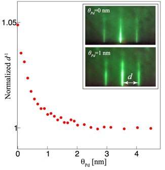
The Pd surface on the Ag(111) was evaluated by RHEED during the deposition. The electron beam was injected from the parallel to the [ ] orientation. Typical RHEED patterns at and 1 nm are shown in the inset of Figure 1. The pattern on the Pd deposited surface was essentially the same as that on the Ag(111), which indicates that the Pd was heteroepitaxially grown as (111). The lattice spacing difference between Pd and Ag is reflected to the (00) to (11) rod distance (d) (indicated as arrows in the image). The Pd surface lattice spacing change was estimated from d–1 as the function of . Dependences of d, which is normalized by d at nm is shown in Figure 1. The observed lattice spacing distribution is in the in–plane direction. The lattice spacing changes from 5% larger Ag to Pd one with , and the mismatch between two is found to fully relax at .
The cross–sectional STEM image of Pd/Ag/Si is shown in Figure 2. The Ag/Si interface is clearly held. The Ag(111) substrate for the Pd film in this study was not the bulk single Ag(111) crystal surface, but it was the Ag(111) film grown on the Si substrate. Therefore, we anticipated that the Pd silicide could be formed near the Ag/Si interface, if the Ag coating on the Si substrate was not perfect. Fortunately, 90 nm thick Ag film perfectly disturbed the Pd silicide formation, and the ideal Ag/Si interface structure was observed. A clear Pd/Ag interface is also observed with the contrast difference. The details of the Pd/Ag interface structure were observed with TEM.
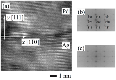
The lattice resolved TEM image near the Pd/Ag interface is shown in Figure 3A. The Pd/Ag interface is located horizontally near the center of the figure (y = 0). The lattice spacing of the Pd and Ag layers were investigated from the FFT image of the lattice image. FFT patterns at the Pd and Ag regions are shown in Figure 3C & 3D respectively. To escape the interface effect,
and
was selected to FFT for (b) and (c), respectively. The spots distance ratio between cross and longitudinal directions matches to
at the both regions, which reflects of the fcc structure projected along [
]. The spots distance at the Pd region is 5% larger than that at the Ag region by reflecting of the lattice spacing difference between two.
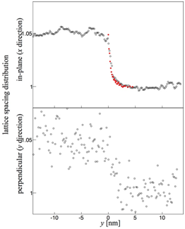
At the very near interface, the lattice spacing was modified from that in the bulk region, although the atomic periodicity is maintained. The lattice space distributions in y direction estimated from the FFT of the TEM image are plotted in Figure 4. In order to measure the local lattice spacing at each y position, the TEM image was sliced into ∼0.5 nm width rectangular shapes in the parallel direction to x–axis. The FFT spots distances of each sliced image are measured in the in–plane direction (upper panel) and in the perpendicular direction (lower panel). The inverse numbers of the FFT spots distance are plotted. The vertical axes are normalized by the lattice spacing at
. The larger data scattering in the perpendicular direction is caused by less the atomic repetition in y direction in the sliced images. In the Ag layer region (
), the lattice spacing is a 5 % larger than that of the Pd and it is independent to y. In the Pd layer region (
), the lattice spacing is drastically decreased to the Pd one both in–plane and perpendicular directions. The lattice spacing in the in–plane direction measured by TEM image is compared by the in–plane lattice spacing observed by RHEED during the Pd deposition (closed circles in the upper panel). The lattice spacing distributions between two measurements are well consistent. The Pd lattice spacing near the Pd/Ag interface are smoothly relaxed from the Ag lattice constant to the Pd one within 2.5 nm (∼10 ML).
The recovery of the lattice spacing from the Ag to Pd one in Figure 1 was more drastic compared with the previous RHEED measurement by Burland & Dobson5. The initial slope at in our measurement was more than 5 times larger than their result. The accuracy of the distribution is strongly depended on the estimation of the Pd deposition rate. The deposition rate by our Knudsen–cell was stable within a 5% fluctuation during the deposition, and the rate was calibrated with the Pd film thickness by the laser microscope measurement and was double–checked by the cross–sectional TEM image in Figure 2. The error of the estimation in our experiment is less than 10%. The lattice spacing distribution observed by RHEED does not necessarily correspond to the cross–sectional TEM measurement (upper panel in Figure 4), because the stress at the surface atom might be different from the atom into the crystal. The distributions between two measurements were exactly matched, and the lattice spacing at the surface and into the crystal was found to be consistent at the same distance from the interface.

Figure 1 RHEED patterns on Ag(111) surface ( ), and the Pd(111) surface ( ). The (00) to (11) rod distance (d) is plotted as the function of . d is normalized by a distance at the sufficiently large .

Figure 3 Cross–sectional TEM image of Pd/Ag interface with atomic–resolution (a). Typical scan lines parallel to x axis at y = 10, 0.5, and –0.5nm (b). FFT patterns of the TEM image at the Pd and Ag layers are shown in (c) and (d), respectively.

Figure 4 Lattice spacing distribution across the Pd/Ag interface. The lattice spacing in the in–plane direction and the perpendicular directions are shown in the upper and lower panel, respectively. The in–plane lattice spacing change measured by RHEED during the Pd deposition is compared (closed– circles).
According to the perpendicular direction of the lattice spacing (lower panel in Figure 4), the distribution was similar to that in the in–plane direction. The lattice spacing was isotropically expanded near the interface, and was relaxed at y = 2.5 nm. The observed expansion near the interface corresponds to the out–of–plane XRD measurement by Häupl & Wiβmann11 on a 4 nm thick Pd(111) thin film grown on the Ag(111).11 They mentioned that the averaged lattice spacing at a larger film thickness of 13 nm might be smaller of ∼0.2 % than the bulk value. This small difference could not be confirmed within the scattering in the vertical axis. The advantage of the TEM compared with XRD is to have the space resolution in the perpendicular direction.
Concerning the heteroepitaxy, Pd is known to grow pseudo–morphically on Ag(111) with columnar structures.6 The size the column has been reported as 10–20 nm. The contrast modulation of the Pd layer in Figure 2 is considered to be the difference of the grain. Large misfit between Pd and Ag may be partially relaxed at the grain boundary.
We have investigated of the Pd/Ag(111) interface structure to identify the sharpness of the Pd/Ag interface. The lattice spacing near the interface was measured by RHEED during the deposition at room temperature, and the cross–sectional lattice spacing was measured by FFT of TEM image. The lattice spacing was found to isotropically expand at the interface, and it relaxed to the intrinsic Pd lattice spacing at ∼10 ML. The Pd/Ag interface at room temperature growth can be identified at most within 10 ML thick.
I gratefully thank to Professor N. Ikarashi for measuring TEM images.
Author declares there is no conflict of interest.

©2018 Aoki. This is an open access article distributed under the terms of the, which permits unrestricted use, distribution, and build upon your work non-commercially.