From the plane wave expansion method, the energy bands and density of states for optimum band gaps were obtained for diamond lattice formed from GaP, Si, InP, GaAs, InAs, Ge and BaSrTiO3 dielectrics spheres drilled in air, by changing the radius of the spheres in symmetric directions of the irreducible Brillouin zone for normalized frequency. The lattice constants were determined by using wavelengths from 150 nm-1nm. The variation of the band gap widths with the filling factor and the variation of gap of mid gap ratios with dielectric constant were investigated. The largest band gaps of 0.0438 for normalized frequency was obtained for Ge and a gap to mid gap ratio of 11.43% for BaSrTiO3 for closed packed filling factor. Diamond crystal doesn’t give band gaps for materials with dielectric constant less than 4 such as SiO2. The gap to mid-gap ratio increases with increased dielectric constant in the range 4-16 but there is no correlation between gap size and dielectric constant. The highest mid-gap of 0.47935
/2 was obtained for GaP. GaP spheres of radii in the range of 0.161 μm to 0.103mm are practically suitable for the wavelength range 1.55μm-1mm. The mode filed distributions were obtained by guiding a telecommunication wave with 1.55 μm wavelength through a photonic cell formed from GaP spheres in the air with a filling factor of 0.34. There were no complete band gaps for air spheres drilled in these eight dielectric mediums.
Keywords: photonic crystals, diamond photonic crystal, plane wave expansion method, mode filed distributions, band gap, filling factor, gap to mid gap ratio
In a three dimensional photonic crystal, an artificially formed dielectric structure, periodic along three different axes, when electromagnetic waves interact they periodically modulate the dielectric constant. A photonic band gap may form in these directions prohibiting the propagation of photons for energies that lie within the gap. Under certain conditions, there will be regions of forbidden frequencies in all the directions of propagation, creating a complete photonic band gap. These three dimensional photonic crystal with complete photonic band gap, which prohibit propagation of light in any three-dimensional directions for any polarization states, are crucial to full control of light-matter interactions and are significant for optical or optoelectronic device operation in radio to optical wavelengths.1 This is an energy band in which optical modes, spontaneous emission, and zero point fluctuations are all absent.2
The possibility of a three dimensional photonic band gaps in periodic structures was suggested by Yablonovitch in 1987,3 one century after Lord Rayleigh (1887) described the one dimensional photonic band gap.4 Once the first three-dimensional photonic crystal with diamond structure was predicted in 1990 by Ho et al.,5 the development of photonic crystals with a complete band gap has advanced from the concept to fabrication from the simple two-dimensional or three dimensional (3D) structures to more complicated 3D structures. Among the various structures, diamond structure is one of the most attractive classes of structures, which consists of two interpenetrating face centered cubic Bravais lattices. Large photonic band gaps have been predicted in all-dielectric crystals with a diamond structure. It is difficult, however, to form three-dimensional diamond structures because the lattice stacking is difficult to achieve compared with simple face-centered cubic or woodpile structure which is a well known simplified diamond structure.5,6 The radius of the spheres can be varied to tune the photonic bands and the spheres do not overlap with each other if the radius is smaller than 0.2165a, where a is the size of the cubic unit cell.7 Edagawa et al.,8 have shown that photonic amorphous diamond also possesses a sizable 3D photonic band gap and that it can confine light at a defect as strongly as conventional photonic crystals can.8
Since for diamond-related structures Korringa-Kohn-Rostoker (KKR) calculations give a lower value for the gap width than the plane-wave calculations,9 the plane wave expansion method applicable to any type of non-dispersive dielectric functions was used as the numerical technique in the present work in modeling and simulating the band structures of three dimensional photonic crystals with diamond lattices formed SiO2, GaP, Si, InAs, GaAs, InP, Ge and BaSrTiO3 spheres drilled in air. For the periodic dielectric function, the magnetic field vector was expanded using Bloch theorem leading to eigenvalue equation in matrix form. A standard eigenvalue equation was solved for the lattice geometries and the energy bands and density of states were calculated in
direction of the Brillouin zone for the eight materials by defining the number of plane waves as 343 for the reciprocal grid. The radius of the dielectric sphere R was changed until an optimum band gap was obtained was obtained. Only the band gaps and density of states for Ge and GaP having largest band gaps are presented. The effects of the parameters on the band gaps were studied. For the propagation of telecommunication waves in the diamond photonic crystal formed by GaP spheres of radius R=0.22a (Closely packed situation) in the air with a filling factor of 0.34, the variation of the amplitude of the electric and magnetic field components relative to X-Z plane obtained using finite difference time domain method are presented.
Plane wave expansion method
The propagation of light in a photonic crystal is governed by the four Maxwell equations. By combining the source-free Faraday’s and Ampere’s laws at a fixed angular frequency
that is with harmonic time dependence of the electric field and magnetic field strength leads to the master equation for a periodic dielectric structure.10 Here, photonic crystal is considered to be a macroscopic, homogeneous, isotropic dielectric material (µ(r)≈1) with no placed charges or current densities with real dielectric constant
and no dispersion. In the plane wave expansion method, a set of plane waves is used to expand, periodic functions in a Fourier series. Because of the periodic nature of photonic crystals, the magnetic field is expanded into a sum of plane waves in reciprocal space giving an arbitrary spatial frequency call reciprocal lattice vector
in terms of basis vectors
in the reciprocal space and set of are integers
. The dielectric function of the structure is similarly expanded in terms of reciprocal lattice vectors and the master equation can be written as:10-12
(1)
The two unit vectors
and
which are perpendicular to
vector, had to be calculated. Fourier transformation of the dielectric function can be further simplified to,
(2)
f is the filling factor, defined as the fraction of area occupied by the localized medium in one unit cell.
and
refer to the dielectric constants of the localized medium and background respectively. The factor
rely on the geometry of the localized medium and the lattice structure. The structure factor for a diamond lattice formed from spheres of radius R is given by:12
(3)
Any two different modes will be orthogonal to each other i.e.
and degenerate modes are not necessarily orthogonal. When a wave with constant wavelength propagates through a photonic crystal it will modulate by the periodicity in that crystal, so the wave will have different filed distributions around the localized regions. Fundamentally, there are two polarizations called the transverse D field and the transverse H field.12
Energy bands and density of states
The diamond lattice is constructed with two interpenetrating FCC lattices, displacing along the body diagonal of the cubic cell by one-quarter the length of the diagonal. It can be considered two spherical atoms in the unit cell. The diamond crystal structure and irreducible Brillouin zone are presented in Figure 1a. The primitive lattice vectors given in term of the lattice constant “a” are
and the locations of two primitive cells are
and
. The symmetric points
and
of the irreducible Brillouin zone are shown in Figure 1b. The diamond photonic crystal was formed by replacing the atoms in the primitive cell with dielectric spheres in air as shown in Figure 1c so that the dielectric constants of localized media
and background material
or drilling air spheres in dielectric mediums (
and
) and the number of grid points n in the direction of each basis lattice vector in space were specified in a three dimensional grid. The number of grid points or plane waves used was
. Defining the number of plane waves as 343, the reciprocal grid was formed. After specifying the high symmetrical points in the three dimensional geometry, all the coefficients in the matrix was formed by calculating two unit vectors. Lattice constant was taken as one
. The radius of the dielectric sphere R was changed until the closed packed filling factor of 0.34 was obtained. For air holes in all the dielectric materials no complete band gaps were found. SiO2
dielectric spheres in air do not give any complete but it gives a partial band gap between second and third band. For the diamond lattice formed from dielectrics GaP, Si, InP, GaAs, InAs, Ge and BaSrTiO3 spheres drilled in the air, the energy bands and density of states for optimum band gaps were obtained by changing the radius of the spheres in symmetric directions
of the irreducible Brillouin zone for normalized frequency
for closed packed filling factor. Ge has the highest band gap relative to other materials. The energy band diagram and density of states for the Ge with a band gap of
between second and third bands and gap to mid-gap ratio
of 10.13% is shown in Figure 2a. The yellow region indicates a complete gap. There are partial band gaps between seventh and eighth and eighth and ninth bands. Figure 2b shows the energy bands and density of states of GaP
with a complete band gap
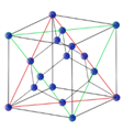
Figure1a Diamond real space lattice.
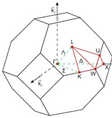
Figure 1c Diamond lattice formed by dielectric spheres.
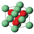
Figure1a Diamond real space lattice.
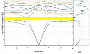
Figure 2a Band diagrams (left) and normalized density of states (DOS) (right) of Ge
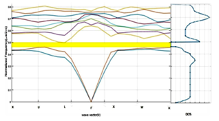
Figure 2b Band diagrams (left) and normalized density of states (DOS) (right) of GaP (11.1).
|
Material
|
Dielectric constant
|
Lattice constant µm
|
Radius of the sphere µm
|
Band gap
|
Gap to mid gap frequency ratio
|
between second and third bands and the gap to mid gap frequency ratio
is Si has a complete band gap of
between second and third band and the gap to mid-gap ratio
is 8.21% .There are partial band gaps between third and fourth band and fourth and fifth band for both GaP and Si lattices. InP has a band gap of
between second and third band and gap to mid-gap ratio
of 9.04%. There are partial band gaps between fourth and fifth bands, eighth and ninth bands and ninth and tenth bands. For closed packed filling factor GaAs and InAs only gives a complete band gap
and 0.161µm between second and third bands respectively. The gap to mid-gap frequency ratios
are 9.06% and 9.85% respectively. There are partial band gaps between fourth and fifth bands, eighth and ninth bands and ninth and tenth bands for both GaAs and for InAs the partial band gaps are between fourth and fifth, ninth and tenth and tenth and eleventh bands. BaSrTiO3 shown in Figure 2c has very large dielectric constant of 200 and it has a narrow band gap of
between second and third bands with gap to mid-gap ratio
of 11.43%.
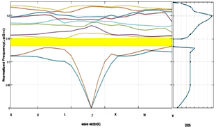
Figure 2c Band diagrams (left) and normalized density of states (DOS) (right) of BaSrTiO3 (200).
From these energy band diagrams, gap width to mid-gap width ratio was obtained for telecommunication λ= 1.55µm wavelength and the lattice constants were calculated from the mid-gap position
for closed packed filling factor. The lattice constants, the radii of the sphere and with the width to mid-gap ratio
for these materials are tabulated in Table 1.
Diamond crystal doesn’t give band gaps for materials with dielectric constant less than about 4 such as SiO2. Figure 3 shows the variation of gap to mid-gap ratio
with dielectric constant in the range 2-16. The gap to mid-gap ratio increases with the dielectric constant, the highest ratio given by BaSrTiO3 of 11.43%, but its band gap is less than the band gaps of other dielectrics and is in the lower region of the band diagram. If this BaSrTiO3 crystal is used for telecommunication wavelength, then the dielectric spheres must be of radius 47.6 nm. Therefore, to design such a photonic diamond crystal is very difficult. Out of all the dielectric materials, Ge with the highest band gaps
of 0.0438 it the most suitable for controlling the electromagnetic waves. GaP with radius of spheres of 0.161µm have the highest mid gap frequency of
. If GaP is used in microwave region then the lattice constant, a must lie in the range 0.47935 nm to 0.47935 m. This range is practically suitable in designing photonic crystals so that Gap with diamond structure can be used in microwave applications. The optimum band gap, for the closed packed filling factor of 0.34 of the diamond structured photonic crystals formed from GaAs, GaP, InP and BaSrTiO3 spheres in the air for the wavelength range 1550nm-1mm is given in Table 2.
|
Material
|
Dielectric Constant
|
Lattice Constant µm
|
Radius of the Sphere µm
|
Band Gap
|
Gap to Mid Gap Frequency Ratio
|
|
GaP
|
11.1
|
0.743
|
0.161
|
0.0375
|
7.82%
|
|
Si
|
11.68
|
0.729
|
0.1578
|
0.0386
|
8.21%
|
|
InP
|
12.41
|
0.7128
|
0.1543
|
0.0398
|
9.04%
|
|
GaAs
|
13.1
|
0.6983
|
0.1512
|
0.0408
|
9.06%
|
|
InAs
|
14.6
|
0.67
|
0.1451
|
0.0426
|
9.85%
|
|
Ge
|
16
|
0.64697
|
0.14
|
0.0438
|
10.13%
|
|
BaSrTiO3
|
200
|
0.2196
|
0.0476
|
0.0162
|
11.43%
|
Table 1 Lattice parameters, dielectric constants and band gaps for telecommunication wavelength for closed packed filling factor of 0.34
|
Dielectric Material
|
Mid-Gap
|
Range of the Lattice Constant
|
Range of Radius of the Sphere
|
|
GaP
|
0.4794
|
0.7430 µm-0.4794 mm
|
0.1609 µm-0.1038 mm
|
|
Si
|
0.4703
|
0.7290 µm-0.4703 mm
|
0.1578 µm-0.1018 mm
|
|
InP
|
0.4599
|
0.7128 µm-0.4599 mm
|
0.1543 µm-0.0996 mm
|
|
GaAs
|
0.4505
|
0.6983 µm-0.4505 mm
|
0.1512 µm-0.0975 mm
|
|
InAs
|
0.4323
|
0.6700 µm-0.4323 mm
|
0.1451 µm-0.0936 mm
|
|
Ge
|
0.4174
|
0.6470 µm- 0.4174 mm
|
0.1400 µm-0.0904 mm
|
|
BaSrTiO3
|
0.1417
|
0.2196 µm- 0.1417 mm
|
0.0476 µm-0.0307 mm
|
Table 2 Optimum band gap the range of radius of the sphere for diamond structure for wavelength range 1550nm-1mm
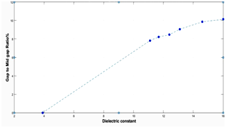
Figure 3 Gap to mid-gap ratio
with dielectric constant.


