International Journal of
eISSN: 2573-2838


Research Article Volume 4 Issue 1
1Department of Physics, Universiti Teknologi Malaysia (UTM), Malaysia
2Department of Physics, University of Mosul, Iraq
3Malaysia-Japan International Institute of Technology (MJIIT), Universiti Teknologi Malaysia (UTM), Malaysia
4Department of Material, Manufacturing and Industrial Engineering, Universiti Teknologi Malaysia, Malaysia
Correspondence: Raja Kamarulzaman Raja Ibrahim, Department of Physics, Universiti Teknologi Malaysia (UTM), 81310 Johor Bahru, Johor, Malaysia
Received: January 28, 2018 | Published: February 21, 2018
Citation: Younus MH, Khalajabadi SZ, Abu ABH, et al. Synthesis and characterization of nanocrystalline silicon carbide thin films on multimode fiber optic by means 150MHz VHF-PECVD. Int J Biosen Bioelectron. 2018;4(1):30–33. DOI: 10.15406/ijbsbe.2018.04.00093
Nanocrystalline Silicon carbide thin films were deposited using 150 MHz very high frequency plasma enhanced chemical vapor deposition (VHF-PECVD) system on the Multimode optical fiber (MMF). The mixture of methane (CH4) and silane (SiH4) as reactive precursor gases and H2 as a carrier were used. The effects of deposition time on the bonding energy, composition and microstructural characteristics of SiC thin films were investigated using FTIR, EDS and FE-SEM. The results reveal that the nanocrystalline SiC films were successfully deposited on the MMF. The thickness of SiC films increased from 54 nm to 1.56 μm as the deposition time is increased from 1 to 3 minutes. The sensitivity of MMF increased from 1.825dB/UIR to 7.341dB/UIR by the 1min deposition time of SiC. Thus, the 150MHz VHF-PECVD seemed to be a suitable technique for coating nanocrystalline SiC thin films and enhancing the sensitivity of the MMF.
Keywords: VHF-PECVD, Optical fiber sensor, nanocrystalline, SiC, deposition time
VHF-PECVD, very high frequency plasma enhanced chemical vapor deposition; MMF, multimode optical fiber; SiC, silicon carbide; Si Silicon; HW-CVD, hot wire chemical vapor deposition; RF-PECVD, radio frequency plasma enhanced chemical vapor deposition; OTDR, optical time domain reflectometer; FTIR, fourier-transform infrared; AFM, atomic force microscopy
In recent years, a number of advantages such as modification of nano-crystalline thin films, the ability for low-temperature deposition processes, the controlling of process, as well as high efficiency and repeatability of process, were offered using plasma deposition technique.1 Silicon carbide (SiC) as a leading candidate for the replacement of Silicon (Si) for high-temperature and power electronic devices has attracted more attention due to its mechanical robustness and chemical inertness at elevated temperatures.2,3 It also becomes an attractive and promising material for fabricating high-temperature pressure sensors. Furthermore, the wide band gap, a high-breakdown electric field, fast response time, mechanical strength and a low leakage current of SiC made it a better material than silicon in high-temperature electronic applications.4-8 In addition, the semiconductor coating layers such as SiC and Si have features apart from sensitivity enhancement of the optical fiber, such as fiber protection, tunability of the resonance wavelength region and bio-chemical compatibility of the sensor.9,10 According to a study reported by Kumar et al.3 the performance of an optical fiber sensor fabricated using surface plasmon resonance (SPR) technique can be enhanced by using silicon carbide (SiC). Nowadays, the plasma enhanced chemical vapor deposition (PECVD),11-13 reactive magnetron sputtering 14, hot wire chemical vapor deposition (HW-CVD)15 and radio frequency plasma enhanced chemical vapor deposition (RF-PECVD) systems 16 are common techniques that are used to grow the nanocrystalline SiC films. PECVD is the most widely used method for the growth of the SiC thin films because of its lower working temperature compared to the other techniques.
Over the decade, a different range of plasma excitation frequencies has been developed to determine the optimum condition to synthesize high quality thin films of nanocrystalline SiC with using PECVD. These researches were more focused on the application of low, medium and high frequencies such as 13.56 MHz, 27.12MHz and 60MHz.6,16-19 According to the author’s knowledge, the use of a very high frequency (VHF) PECVD at 150MHz to grow nanocrystalline SiC films on the multimode optical fiber (MMF) has not been reported elsewhere. In this paper, the growth of the nanocrystalline SiC thin films on the MMF using VHF-PECVD at 150MHz excitation frequency was performed. The effect of various deposition times on the microstructure, thickness and homogeneity of SiC thin films on the MMF was investigated using FE-SEM. The elemental analysis, composition, and the bond structure of the deposited SiC films were studied using EDS and FTIR. The sensitivity of MMF was measured by the Optical Time Domain Reflectometer (OTDR) technique.
The SiC films were deposited on the MMF using a VHF-PECVD system at a substrate temperature of 25°C. The plasma-excitation frequency of the system was 150 MHz. Silane (SiH4, 99.9995%) and methane (CH4, 99.999%) gases were used as reactive precursor gases for SiC thin films deposition, while the carrier gas was the hydrogen (H2, 99.999%). The SiH4 flow rate was adjusted at 2 sccm, the CH4 flow rate at 20 sccm, H2 flow rate at 25 sccm, total pressure at 9 x10⁻² Tor and plasma power density at 20 W. The deposition times were fixed at 1, 2 and 3 minutes. A Perkin Elmer (SP8000, UK) Fourier-transform infrared (FTIR) spectrometer was used to determine the functional groups of the deposited films. The surface morphology, the film thickness and cross-section images of the deposited SiC films were observed using a field emission scanning electron microscopy (FE-SEM JEOL JSM-5800 LV) equipped with an energy dispersive (EDS) X-ray spectrometer. The elemental analysis of the deposited films was performed using EDS. The surface topography and roughness of the deposited SiC films by 150 MHz VHF-PECVD were examined by Atomic Force microscopy (AFM). The Optical Time Domain Reflectometer (OTDR) technique was introduced to measure the return loss of the MMF sensor with and without the SiC coating. The sensitivity in term of the return loss per unit of refractive index (dB/UIR) of the MMF was determined with different refractive indices ranging from 1.440– 1.474 of pure liquid Cargille solutions.
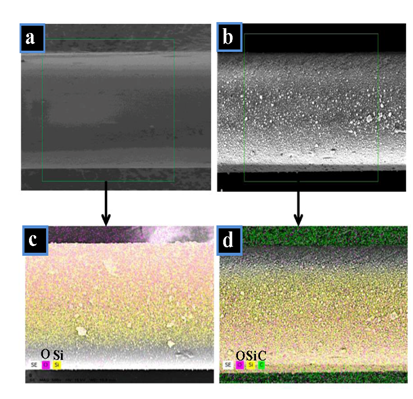
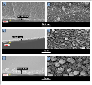
Figure 1 displays the typical EDS spectra of MMF before and after SiC deposition. It shows that the Si, C and O elements are detected after different deposition times. The EDS results of the SiC films deposited at 1, 2 and 3 minutes are mainly composed of Si, C and O (Figure 1B-1D), while the EDS spectra of MMF without SiC is composed of only Si and O as shown in Figure 1A. It should be noted that the EDS detection of the C spectra as well as the decrease of in the O intensity confirm the substantial growth of SiC films on MMFs. Figure 2B shows the elemental mapping of MMF before and after 1 min of SiC deposition. The synthesis of SiC film with uniform thickness can be observed in Figure 2B. As can be seen in Figure 2A, there is no C element on the surface of MMF before SiC deposition. Images (a), (c), and (e) in Figure 3 present the cross section of the MMF sensor coated with SiC film at different deposition times of 1, 2, and 3 minutes, respectively. Images (b), (d), and (f) in Figure 3 present the surface morphologies of MMF sensor coated with SiC film at deposition time of 1, 2, and 3 minutes, respectively. It can be seen that a continuous and uniform film of SiC is deposited on the MMF using 150 MHz VHF-PECVD (Figure 3A & Figure 3C & Figure 3E). The FE-SEM images reveal the dependent of morphology of the SiC film on the deposition time. As shown in Figure 3A, at the deposition time of 1 minute, the thin film of SiC is created and covered the entire cross section of MMF sensor with thickness of 54.06 nm.


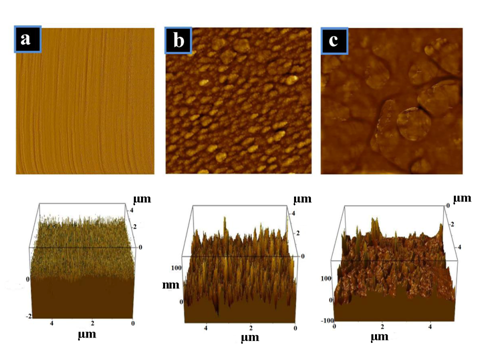
Figure 3B depicts the smooth surface morphology of the SiC film consisting nanoparticles with ~30nm particle size that deposited on the MMF sensor at 1 minute deposition time. The extension of the deposition time to 2 and 3 minutes increase the thickness of the deposited SiC films to 531.2 nm and 1609 nm (Figure 3C & Figure 3E), respectively. The surface of the SiC film becomes rough as the number of SiC granules has increased. By increasing deposition time, the small nanoparticles of SiC films tend to form agglomerates that reduced the homogeneity of particle size of the deposited films as shown in Figure 3D and Figure 3F. However, the porosity of the particles deposited films also decreased with increasing deposition time, and as a result, the SiC films become more compact. It can be concluded that the SiC film at deposition time of 1 minute is very smooth and thin that almost covered the whole length of the MMF sensor which can be useful to enhance the sensitivity of the MMF. Whereas, the thicker SiC films at deposition time of 2 and 3 minutes has a strong tendency to form agglomerates, which can affect the performance of the MMF sensor. Figure 4 shows the high-resolution AFM images of the surface topography for the MMF sensor with and without SiC at scanning area size (5X5 µm2). Figure 4A shows the MMF without SiC with average surface roughness Rrms= 1.13039 nm. Image in Figure 4B shows the deposited SiC film on the MMF at 1 min deposition time with average roughness surface Rrms= 2.76005 nm while image in Figure 4C shows the deposited SiC on the MMF at 3 min deposition time with average roughness Rrms= 15.535 nm. It can notice that the roughness of SiC surface is increases as the deposition time is extended. Furthermore, the surface microstructure of SiC is spherical which supports the results that obtained from the FE-SEM image; however, the cross-sectional images show the columnar growth of SiC particles in nano-scale were obtained using 150 MHz VHF-PECVD.

Figure 5A shows the FTIR absorption spectrum of the MMF sensor before and after the SiC deposition. The peak at 800 cm−1 is assigned to SiC bond.20-22 The presence of SiC bond clearly confirms the formation of SiC film on the MMF sensor. Figure 5B illustrates only the SiC spectra, which clearly shows that by increasing of deposition time, the intensity of SiC peak also increased indicating the increasing amount of deposited SiC films. The peak at 930-1000 cm−1 is due to the wagging and vibration mode of the C–H bond.21 FTIR band at ~1210 cm−1 represents the vibration mode of the Si-O bond.21,23 The peaks at 1335 and 1424 cm-1 are the symmetric modes of the C-H3 and Si–O absorption bands, respectively.24,25 The Raman analysis also indicates the formation SiC films by 150 MHz VHF-PECVD method (Figure 6), as the spectra are appeared at 766 cm−1 and 976 cm−1 wave numbers that represent presence SiC films on the surface MMFs. Increase of intensity of Raman spectra at longer deposition times describes the synthesis of larger amount of SiC. These results are consistent with FTIR spectroscopy analysis. Figure 7 shows the return loss of MMF sensor with and without SiC coating versus different refractive indices of the Cargille solutions. The MMF coated SiC shows the higher return loss than the uncoated MMF that indicates the increase in sensitivity of SiC coated MMF. The maximum values of sensitivity of MMF without and with SiC (i.e. return loss per unit change in refractive index) were found to be 1. 825 dB/UIR and 7. 341 dB/UIR, respectively. Overall, results show that the interactions of different refractive index of the Cargille solutions with SiC films make the sensor highly sensitive when compared to the uncoated MMF.
Referring back to the FTIR, EDS and RAMAN analysis as well as FE-SEM and AFM images, it can be deduced that the SiC films were successfully deposited on the surface of MMF using 150MHz VHF-PECVD. However, increasing deposition time would also increase the amount of SiC coating and the number of SiC agglomerates. The sensitivity of MMF was found to significantly increase by the1 min SiC deposition.
The authors want to thank and appreciate the staff at the Laser Center, University Technology Malaysia (UTM) for providing research facilities required to complete this study. The authors gratefully acknowledge for financial support research of Grant No. 4F648 as well as the contract research Grant No. R.J130000.7826.4F869, Q.J130000.2526.13H67.
The author declares no conflict of interest.

©2018 Younus, et al. This is an open access article distributed under the terms of the, which permits unrestricted use, distribution, and build upon your work non-commercially.