International Journal of
eISSN: 2573-2838


Research Article Volume 3 Issue 1
Department of Electric and Computer Engineering, Marquette University, USA
Correspondence: Ronald A Coutu Jr, Department of Electrical and Computer Engineering, 1627 W Wisconsin Ave, Milwaukee WI, USA
Received: July 28, 2017 | Published: September 6, 2017
Citation: Coutu RAJ, Tomer D. Micro-contacts testing using a micro-force sensor compatible with biological systems. Int J Biosen Bioelectron. 2017;3(1):215–222. DOI: 10.15406/ijbsbe.2017.03.00052
This paper presents the performance and reliability testing of microelectromechanical systems (MEMS) switches by using a micro-force sensor which was originally designed/used to conduct mechanical testing of biological cells. MEMS switches are key components for radio frequency (RF) applications due to their extremely low power consumption and small geometries over conventional technologies. However, unstable electrical contact resistance severely degrades the performance and reliability of such micro-switches. Therefore, our focus is to improve the performance and reliability of “cold” switched micro-contacts by using novel contact materials and engineered micro-contact surfaces. The contact metallurgies considered in this work are “similar” thin film combinations of Au, and composite Au/CNT. The non-engineered switch consists of a metallic hemispherical bump and a planar sheet as upper and lower contacts, respectively. On the other hand, the engineered switches have 2D pyramid structure in lower contacts while having a hemispherical bump at upper contact. Hemisphere on planar, Au-Au, contact pairs resulted in initial contact resistance (RC) values of ~0.1Ω (FC=200µN) that linearly increased to ~1.0Ω after ~10×106 cycles and then failed open (~10.0Ω) at ~20×106 switching cycles. The Au-Au/CNT composite, hemisphere on planar contact pair showed similar RC performance with extended reliability (~40×106 switching cycles) when the composite film was integrated into the lower planar contacted. Upper hemisphere on the 2D pyramid, Au-Au, contact pairs resulted in initial RC values of ~0.9Ω (FC=200µN) that linearly decreased to ~0.5Ω at >10×106 cycles (not failed). This work suggests that the combination of engineered lower contacts and composite materials can significantly improve the performance and reliability of micro-switches.
Keywords: biosensors, micro-switch, micro-contacts, engineered contacts, gray-scale lithography
In recent years, manipulation and mechanical testing of fragile biological cells have emerged as an important research area.1 In biocellular systems, force varies from few µN to pN depending on bonding type (covalent, noncovalent etc.) which requires a precise control and accurate detection of force to avoid physical damage to cells.1-3 The use of microcantilevers as a force sensor is a well-established method to detect forces from 100 mN down to several pN with a precise manipulation of micro- and nano-seized objects.4 In his review article, Raiteri et al.5 have summarized the use of micromechanical cantilevers in various biosensing experiment.5 Similarly, Sun et al. have demonstrated the use of monolithic micro-gripper with two axis force feedback to perform µN-nN force controlled manipulation of biological cells.1,6 Similar to biological cells, microelectromechanical systems (MEMS) switches are also fragile components and operate in mN- to nN- force, therefore, demands ultra sensitive force sensors for characterization.
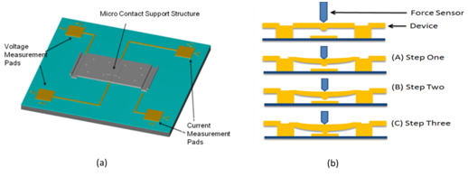
MEMS switches are key components for radio frequency (RF) applications due to their extremely low power consumption and small geometries over conventional technologies.7,8 However, their poor performance and shorten lifetime has been attributed to fluctuations in contact resistance values. Often, micro-switch reliability research focuses on improving the mechanical switch design and not investigating the micro-contact region. In our opinion, this approach is an attempt to “engineer away” poor micro-contact performance and/or reliability with a superior switch design. We believe the micro-contact is the real culprit and needs to be studied directly before significant micro-switch reliability strides can be realized. In this work, the performance and reliability of planar and engineered micro-contacts constructed from novel materials such as Au and Au/CNT composite are studied directly after decoupling the electrical contact from the mechanical design. Here, micro-contact metallurgies considered were “similar” thin film combinations where, “similar” contacts mean having the same material in the upper and lower contacts. All the micro-contacts have same geometries; a hemispherical bump at upper and planar or engineered (2D pyramid) structure at lower contact. The performance and reliability of micro-switches are investigated in a novel test fixture which is made of microelectronics grade plexiglass materials so that tests can be conducted in controlled dry N2 (99.999%) environment. This test fixture is capable of both “hot” and “cold” switched single contact and cycled contact testing up to 3KHz. Furthermore, it allows to collect the contact force (FC) and resistance (RC) data while applying a calibrated µN load to a MEMS micro-contact support structure in the Holm cross-rod configuration shown in Figure 1.9 The detailed information about test fixture and micro-contact fabrication is given in materials and methods section followed by results and discussion of various micro-switches.
Micro-contacts test fixture
In the past, various test fixtures such as atomic force microscopes (AFM), scanning tunneling microscopes (STM), and nanoindenters were used to collect the micro-switch data (i.e. RC and FC) to determine their performance.10-14 These methods, however, have some severe limitations. For example, one can perform life cycle testing of MEMS switches with these methods but cannot measure contact force. The newer versions of these test fixtures allow contact force measurement but at extremely low cycle rates (i.e. 10-100 Hz). Therefore, we designed a novel test stand specifically to gather data under controlled test conditions at high cycle rate (up to 3 kHz).15 This test stand can apply a known contact force throughout all stages of the experiment and obtain RC from current and voltages measured by using NI-4070 flex DMM module. Furthermore, the actuation position was controlled with a Thorlab PAZ005 actuator, and the force was measured using a FemtoTools model FT-5270 force sensor. The tests were conducted on a vibration isolation table in a dry N2 (99.999 %) environment that allowed the manipulation of the micro-contact and the ability to in-situ monitor the contact throughout testing. A picture of the complete test fixture is shown in Figure 2.
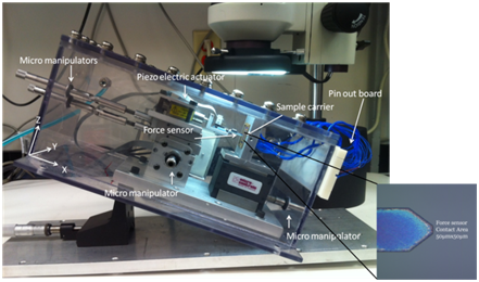
Using this test stand, FC and RC were simultaneously measured during two test profiles, an initial contact test (ICT) and a cold switch test (CST).9,16 During ICT, an external point load was applied to the top surface of the micro-contact support structure while sensor displacement and force were monitored during support structure deflection. Once electrical contact was initiated between the upper and lower contact surfaces, the measured force is classified as contact force. For this work, ICT profiles were conducted for every cycle where a contact resistance measurement (i.e. Rc versus FC) was required. During testing, the system was automated to increment the force sensor position, in nanometer-sized fixed steps, until the force sensor limit was reached. Since the micro-contact support structure required approximately 1mN of force to fully deflect, the available sensor force for each contact resistance measurement was approximately 1mN. On the other hand, during CST profiles the force sensor displacement needed to apply approximately 200µN of force to close the micro-contact and then current was applied across the micro-contact to simulate use. During this test, the current was applied only once the contact was fully closed and it was then removed prior to breaking contact. These steps are then repeated for the desired number of cycles at a maximum frequency of 3kHz.13-17
Micro-contact support structure (Fixed-Fixed Beam)
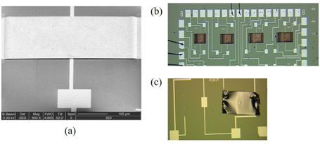
The micro-contact support structure used in this experiment was a MEMS fixed-fixed beam that emulated Holm’s crossed bar experiment, shown in Figure 1, on the micro-scale. This support structure design allows performing four-wire measurement in which current flows through the micro-contact only when contact is completely closed. After then voltage can be measured across the micro-contacts using integrated National Instruments electronics components. The fixed-fixed beams had a width of 150µm and a variety of lengths ranging from 350µm to 500µm. The beams were designed with a hemispherical upper contact bump of diameter 6-8µm, a lower planar contact and a gap distance between the upper and lower contacts of 2µm.16,17 Generally, the lower contacts were evaporated Au (all except for Au-CNT composite films) while the upper contacts were sputtered or reactively sputtered Au. Figure 3 shows a 3D model of the fixed-fixed beam micro-contact structure. Figure 4 is a collection of images illustrating a MEMS released beam (Figure 4A), a packaged array of micro-contact support structures (Figure 4B) and an example of “flipped back” beam that was used to image lifecycle tested contacts.
Contact resistance modeling
In the very first modelling of RC, Holm ignored surface contamination and worked with clean contacts only.9 However, such assumption is valid only at macro scale where contact surfaces appears smooth but on the micro/nano scale no contact surface is perfectly smooth. Therefore, it is important to consider the effect of surface contaminations on micro-contact performance. Contact surfaces are comprised of asperity peaks or “a-spots”, which meet at the interface and become the contact area.9,18 These “a-spots” have been described as “small cold welds providing the only conducting paths for the transfer of electrical current”.18 An effective conducting area is used for making simplified contact resistance calculations.18 Majumder et al., modeled micro-contact switches with three steps.13 First, they determined the contact force available from their electrostatically actuated micro switch. This contact force was a function of the device actuation voltage. Second, they determined the effective contact area at the interface as a function of contact force. Finally, they determined the contact resistance as a function of the distribution and sizes of the contact areas.13 Both Majumder and Holm noted that the surface profile was sensitive to plastic and elastic material deformation.9,13 Elastic material deformation modeling is accurate for extremely low values of contact force of a few μN where surface asperities retain their physical shape after the contact force is removed. Plastic deformation results when permanent surface change occurs by the displacement of atoms in the asperity peaks or “a-spots” whereas neighboring atoms are retained under elastic deformation. The “classical” contact resistance model using Maxwell’s spreading resistance theory is:
(1)
Where RC is the constriction resistance, ρ is the resistivity and a is the effective radius due to conducting “a-spots”.9 When the contaminate film resistance is neglected, the constriction resistance is equal to the contact resistance. The “classical” macro switch contact resistance models shown in Equations (2) and (3) relate contact resistance (RC) as a function of contact force (Fc) and other material and geometric quantities. Equation (2) is used to calculate RC for elastic material deformation (RC ∝ FC -1/3) and equation 3 is used to calculate RC for plastic deformation (RC ∝ FC-1/2)
(2)
(3)
Where the contact resistance for diffusive electron transport is represented by RcDE for elastic material deformation and RcDP for plastic material deformation.9 E'is the Hertzian modulus of the contacting surfaces, R is the “a-spots” radius of curvature, H is hardness of the softer contact materials and FC is the contact force.
Novel contact materials
Contact materials also have a major role in determining the performance and reliability of micro-switches. Hardness, as well as conductivity and other material properties influence the contact resistance. Gold, palladium, platinum and alloys are commonly used micro-contact materials due to their high conductivity.8,19 Since these materials are very soft and wear easily, other materials are required to enhance the lifecycle and the performance of the micro-contacts. One of the promising material is gold-carbon nanotube (Au-CNTs) composite. The high Young's Modulus and low resistance of CNTs makes them suitable candidates for micro-switch contacts. For instance, contacts consisting of single-walled CNTs coated with a thin Au layer were shown to have a resistivity between 1- Ωm.20 CNTs have been reported to have an elastic modulus of approximately 1TPa, which is comparable to diamond's elastic modulus of 1.2Tpa.20 Yunus et al.20 explored two contact pairs with carbon nanotubes: Auto multiwall carbon nanotubes (MWNTs), where one electrode is Au and the other is MWNTs coated with a thin Au film so the contact interface is Au-Au.20 Figure 5 shows a cross-section of a micro-contact support device with a hemispherical upper contact bump and a planar lower contact. The novel contact material is located on the surface of the upper contact bump.

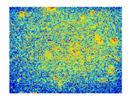
In this study, composite Au-CNT contact layers were fabricated by adding CNTs to the upper hemispherical and the lower planar contacts followed by encapsulating the CNTs with a sputtered gold film prior to deposit the sacrificial layer (lower contact design) or electroplating the structural layer (upper contact design). The CNTs were deposited by spin coating a mixture of CNTs that were suspended in isopropyl alcohol. After depositing the CNTs, a thermal image, shown in Figure 6, was taken to qualitatively evaluate the distribution of the CNTs on the lower contact.15 The more readily identifiable CNT groupings or “clumps” appear as the bright green and red spots, indicating a higher CNT concentration. Image analysis revealed approximately a 55% coverage of the Au-CNT composite film on the lower planar contact area. The addition of CNTs into the lower micro-contact material is theorized to enhance thermal conductivity but it also tends to increase film resistivity since the CNTs disrupt the normal homogeneity of a thin film Au contact.
Engineered contacts using gray-scale lithography
The ability to develop 3D micro-structures is of great importance for increasing optical and electro-mechanical device performance. Previous technologies used multiple direct writing and photolithography steps, or customized equipment.21-25 However, these technologies are restricted to a limited range of shapes and do not utilize batch processing. Gray-scale lithography (GSL) has emerged to develop 3D micro-structures in various materials.25-27 The use of gray-scale technology allows unique 3D shaping to be performed in a single photolithography step with subsequent dry etching for pattern transfer.27 Gray-scale lithography utilizes a “virtual” mask patterned with varying intensities of gray pixels and spacing. This virtual mask is used to control laser intensity in the lithography system. Changing the size of the pattern and the shade of gray, varies the intensity of the laser power; with each distinct power level corresponding to a gray level. The height profile in the photoresist after development (composed of photoresist gray levels) will depend upon the incident intensity, time of exposure, and photoresist contrast. Gray-scale and traditional UV lithography are pictorially compared in.Figure 7
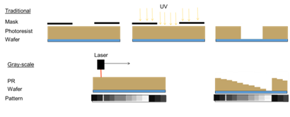
Gray-scale “virtual” masks were designed and used with a Heidelberg µPG101 UV laser lithography system to produce GSL structures in positive photoresist.28 The varying levels were patterned by changing the intensity of the laser, which was controlled by the assigned gray-scale value in the virtual mask design. Due to limitations in controlling the Heidelberg’s UV laser, only 100 out of the total 255 possible gray scale variations were used to produce 100 unique height levels.28 This limitation led to a stepped profile in the photoresist illustrated in Figure 8.28 The resulting gray-scale levels are readily apparent in the photoresist as color variations shown in the optical image below (Figure 8A). The virtual gray-scale lithography mask was incorporated into the overall traditional lithography mask set design by manually aligning the Heidelberg system, using already fabricated device features, to guide where the 2D pyramid areas should be placed. This method was labor intensive, but with the addition of a few actual alignment marks on the wafer, acceptable alignment onto the lower contact pad was possible. Scanning electron microscope (SEM) image of a series 2D pyramid structures, etched into the Si wafer using reactive ion etching (RIE), are shown in Figure 9.
Each micro-contact was initially tested with an ICT to assess performance and then transitioned to CST to assess reliability. During ICT, the current was maintained at approximately 0.02mA, an external load was applied to the contact support structure and the corresponding voltage was measured as the contact force was increased to a preset value (i.e. ~250µN). During CST, a constant current of 46mA and a constant contact force of 200µN were used during the individual measurement cycles.17 This test methodology was necessary to avoid continuous, inadvertent higher power hot switching of the micro-contacts. The devices were then cycled to 107 cycles (or failure) and the data analyzed to evaluate contact evolution. Measurements were made at designated numbers of cycles and set by a measurement interval (10-1000). Between measurements, the micro-contacts were cycled mechanically at the predetermined actuation rate (i.e. 1-3KHz) and contact force (i.e. 200µN). Sensor location was reset during each measurement cycles to avoid excessive position drift during high cycle rate testing.
Au-Au, hemisphere on flat, micro-contacts
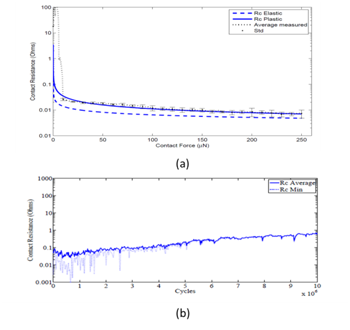
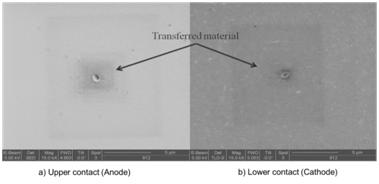
Figure 10 is ICT and CST data for an Au-Au, hemisphere on a flat micro-contact pair.16 The ICT compares modeled values for micro-contact resistance to measured data. The plotted data is an average of 15 ICT measurements; also shown is the standard deviation of that data. Figure 10A shows that at extremely low contact force, less than 10μN, the measured contact resistance is much higher than the model. As the load increases, the average measured values more closely follow the RC plastic model. The initial CST (Figure 10B) RC values of ~0.1Ω (FC = 200µN) linearly increased to ~1.0Ω after ~10×106 cycles and then failed open (~10.0Ω) at ~20×106 switching cycles. Post CST, SEM image of the upper contact bump with corresponding lower planar contact are shown in Figure 11. A small area of wear can be clearly seen after ~107 cycles. This matches the relatively low, stable contact resistance observed throughout the microswitch's lifetime. These data will serve as a baseline when comparing novel contact materials and engineered 2D pyramid lower contacts results. The linearly increasing RC shown in the Figure 10B indicates contaminate film or frictional polymer growth was occurring in the contact region.16 The Figure 11 SEM image, however, does not reveal any noticeable contaminant film growth.
Au-CNT composite upper contact, hemisphere on flat, micro-contacts
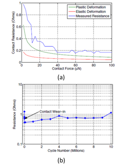
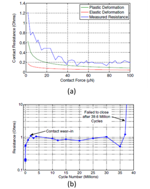
Figure 12 is ICT and CST data for an Au-CNT composite upper contact in a hemispherical on lower planar contact pair.17 The ICT (Figure 12A) compares modeled values for micro-contact resistance to measured data. The plotted data is an average of 15 ICT measurements.Figure 12A shows that at extremely low contact force, less than 40μN of contact force applied, initial contact resistance mimics the plastic deformation resistance model. The offset between plastic model and data could be a result of surface topography or contamination. The CST results Figure 12B show an initial contact resistance at ~1.22Ω until contact wear-in and then a relatively stable contact resistance ranging from ~0.5Ω to ~0.7Ω at ~9×10⁶ cycles. The device failed closed (1.1Ω) at ~107 cycles. Overall, these results are similar to the Au-Au, hemisphere on flat shown in Figure 10.
Au-CNT composite lower contact, hemisphere on flat, micro-contacts
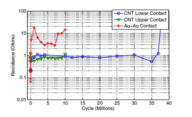
Figure 13 is ICT and CST data for an Au-CNT composite lower contact in a hemispherical on lower planar contact pair.17 The ICT (Figure 13A) compares modeled values for micro-contact resistance to measured data. The plotted data is again an average of 15 ICT measurements. Figure 12A shows that at extremely low contact force, less than 50μN of contact force applied, initial contact resistance mimics the plastic deformation resistance model. The offset between plastic model and data could be a result of surface topography or contamination. The CST results (Figure 13B) show an initial contact resistance at ~0.19Ω until contact wear-in and then a relatively stable contact resistance of ~1.0Ω through ~36.9×10⁶ cycles and then a failed open device at ~39.6×10⁶ cycles (>10.0Ω). These results show similar trending to the Au-Au, hemisphere on flat data provided in Figure 10 the Au-Au contact pair showing better performance through 5×10⁶ cycles and the Au-CNT composite lower contact showing more stable contact resistance up to failure at ~40×106 cycles. Figure 14 is a comparison of lifetime data for three hemispheres on flat contact pairs with three different contact metallurgies: Au-Au, Au-CNT composite upper contact, and Au-CNT composite lower contact.
The Au-Au micro-contact exhibited steadily increasing contact resistance as the number of actuations increased. This particular micro-contact was cycled nearly ~10×106 cycles, at which point the closed contact resistance was ~14.4Ω (i.e. failed open). The CNT composite films, however, in either the lower or upper contact did not display this same steady rise in contact resistance. The micro-contacts with CNTs in the upper contact was also cycled to ~10×106 cycles, at which point the contact failed closed with a resistance of ~1.1Ω. Finally, the micro-contacts with an Au-CNT composite film lower planar contact was cycled to approximately ~40.0×10⁶ cycles with a closed contact resistance of 1.21Ω being measured just before the device failed to open (i.e. high contact resistance). This failure was most likely due to the build-up of an insulating contaminant film. The most promising results were with the Au-CNT composite film in the lower planar contact. This micro-contact pair exhibited much lower and consistent resistance compared to a similarly constructed Au-Au micro-contact pair. This could be a result of the CNTs providing a highly conductive thermal layer to diffuse joule heating and thus allow for a longer lifetime. The Au-CNT film may have also allowed some current to flow through the CNTs, thereby reducing resistance in the contact film. After cycle testing, the Au-CNT composite lower contact was examined to determine the failure mechanism. SEM imagery of the lower contact (Figure 15) revealed an area of contamination had developed while testing this contact metallurgy. To further evaluate the contaminate film, energy dispersive spectroscopy (EDS) data were collected at a relatively low voltage (i.e. 2.185keV) to minimize penetration depth. The resulting SEM image and EDS are shown in Figure 15.
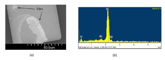
The amount of carbon present on the lower contact was ~20% of the return on the EDS measurement (~1μm in-diameter). We believe that the encapsulated CNTs, where beginning to wear through the thin Au capping layer and the exposed CNTs accelerated contaminant film growth. This rapid rise of resistance is similar to what has been seen in the frictional polymer literature.18 Frictional polymers are organic contaminant films that develop on commonly used contact materials in the presence of organic vapors or compounds found in the operating environment of the contact.18 Based on this, it appears that device failure was caused by exposed carbon fibers that led to the rapid growth of a frictional polymer. Despite this catastrophic failure, the Au-CNT composite lower contact in a hemisphere on flat configuration exhibited approximately 4× increased reliability. Next engineered lower contacts fabricated using gray scale lithography are investigated.
Au-Au, hemisphere on 2D pyramids, micro-contacts
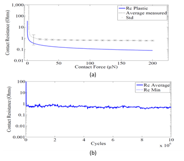
Figure 16 is ICT and CST data for an Au-Au, hemisphere on engineered lower contacts pair (i.e. 2D pyramid area).16 The ICT compares modeled values for micro-contact resistance to measured data. The plotted data is an average of 15 ICT measurements; also shown is the standard deviation of that data. The data shows a very stable contact resistance (i.e. ~1.0Ω) across a wide spectrum of applied contact force values (i.e. ~25µN to ~200µN). This is due to the engineered, fixed geometry 2D pyramid lower contact. Essentially the contact resistance was “dialed in” by imprinting a fix, alternating high/low area onto the lower contact. This hypothesis is supported by Equation 1 that shows the contact resistance is inversely proportional to the contact area through the effective radius (i.e. a) of a conducting “a-spots”.19 The CST results (Figure 16B) show a stable, low contact resistance that linearly decreases from ~0.9Ω to ~0.5Ω up to 107 switch cycles. These results support the thesis that developing contaminant films are being actively shed off conducting area into the “valleys” of the lower contact. The CST test was halted to maintain test data consistency not because the micro-contact failed. The data presented, thus far, in the sections (A-C) were composed of either Au-Au or Au-CNT composite contact materials with either hemisphere on flat or hemisphere on 2D pyramids. So far all of the load polarities set to the upper contact as the anode and the lower contact as the cathode.
Au-Au, hemisphere on flat, micro-contacts (polarity swap)
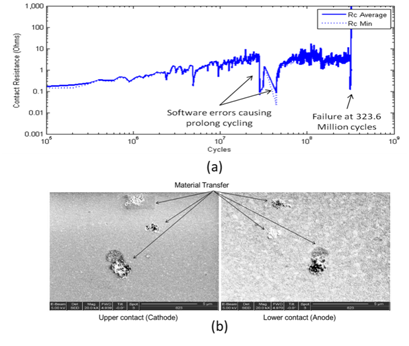
The CST results (Figure 17) for an Au-Au, hemisphere on the flat set of micro-contacts showed approximately a 32× improvement in device reliability (~0.323×10⁹ switch cycles before failure) with the upper contact being the cathode and the lower contact being the anode. This configuration has opposite load polarity to that previously tested in Section A where device failure occurred at ~107 switch cycles (Figure 10). Recall from fabrication discussion in Section 2B that the Au-Au micro-contact support structure was fabricated with an evaporated Au lower contact and a sputtered Au upper contact. Results show that sputtered films tend to be slightly harder and more resistive than evaporated films because of their smaller, tighter grain structures.19 This can be observed in Figure 17 where the upper contact (i.e. sputtered Au) has tightly packed grains and the lower contact (i.e. evaporated Au) is more columnar and less tightly packed together.19 Figure 17B also shows contact wear and material transfer that ultimately caused the device to fail closed (> 1KΩ).
In this work, a micro-force sensor that is typically used in the mechanical testing of biological cells, is used to investigate micro-contacts. The main advantage with this novel fixture is that the contact force is precisely applied even at higher actuation rates up to 3 kHz. This research illustrates that the performance and reliability of MEMS micro-switches can be significantly improved using unique contact materials (Au on the upper hemispherical bump and Au-CNT composite on lower planar contact) resulting in four times longer lifetime and low contact resistance (0.2Ω). Furthermore, it is demonstrated that engineered lower contacts (i.e. 2D pyramid) result in stable RC with somewhat higher RC values (i.e. 0.9Ω versus 0.2Ω). Overall these improvements will provide benefits to MEMS researchers with lower contact resistance, higher reliability, and lower power consumption. Finally, as critical features in micro-mechanical devices continues to decrease in size, there may be other bio-sensing test methods that can be directly applied to investigating MEMS.
The authors thank the Air Force Office of Scientific Research (AFOSR) for funding this research (# F4FGAO5126J001), and Mr. Thomas Edleman, Mr. Benjamin Toler, Mr. Christopher Stilson and Dr. Tod V. Laurvick, for their participation.
The author declares no conflict of interest.

©2017 Coutu, et al. This is an open access article distributed under the terms of the, which permits unrestricted use, distribution, and build upon your work non-commercially.